
Get asas: litar AND, OR dan NOT
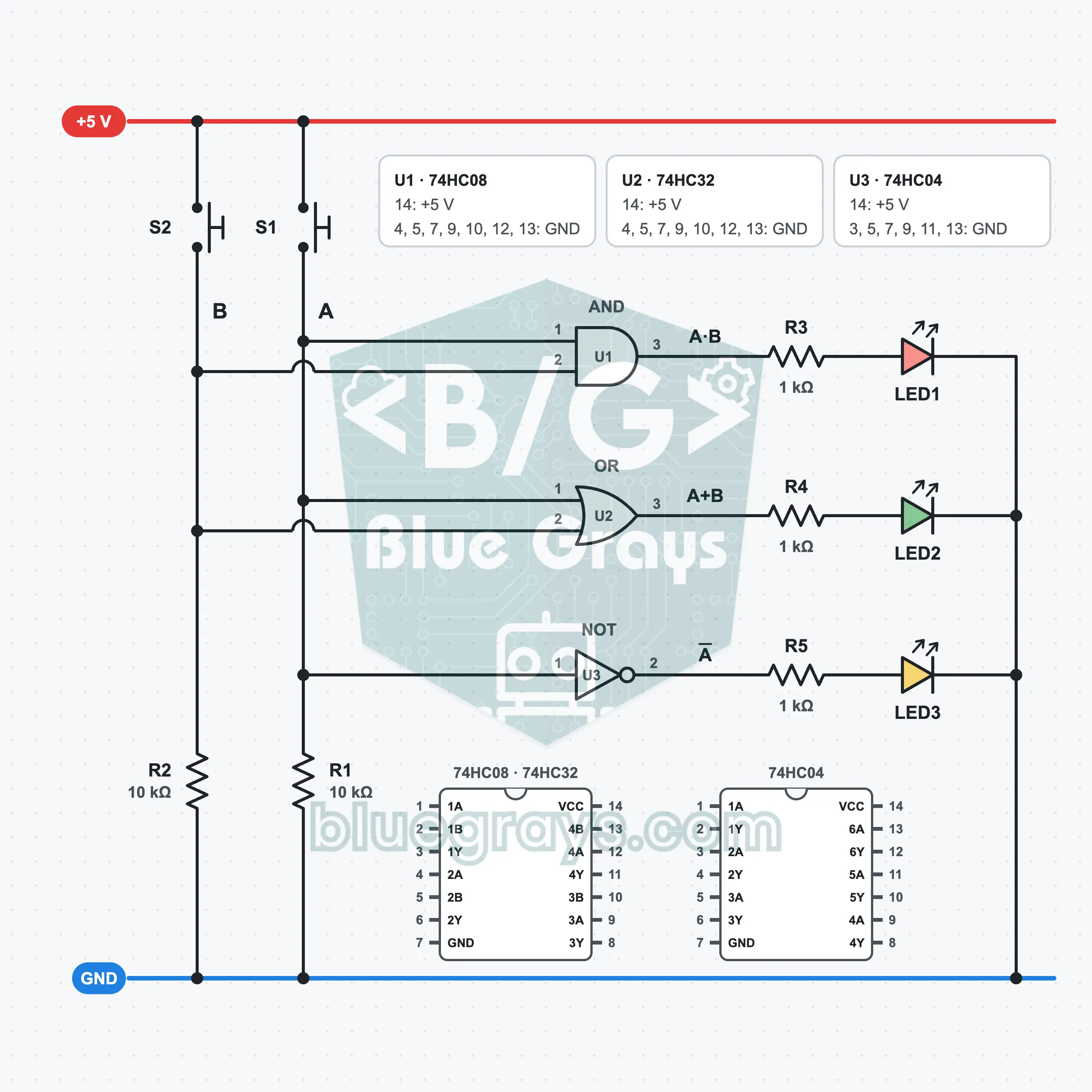
Cuba tiga blok binaan elektronik digital pada breadboard yang sama. Dua butang menjadi input A dan B kamu; LED merah menunjukkan hasil get AND, LED hijau get OR dan LED kuning get NOT. Dengan IC 74HC08, 74HC32 dan 74HC04, kamu mencuba empat gabungan butang satu demi satu dan menghasilkan jadual kebenaran dengan mata sendiri.
Video
Gambar Rajah Litar
Susun Atur Breadboard
Langkah Pemasangan
- 1
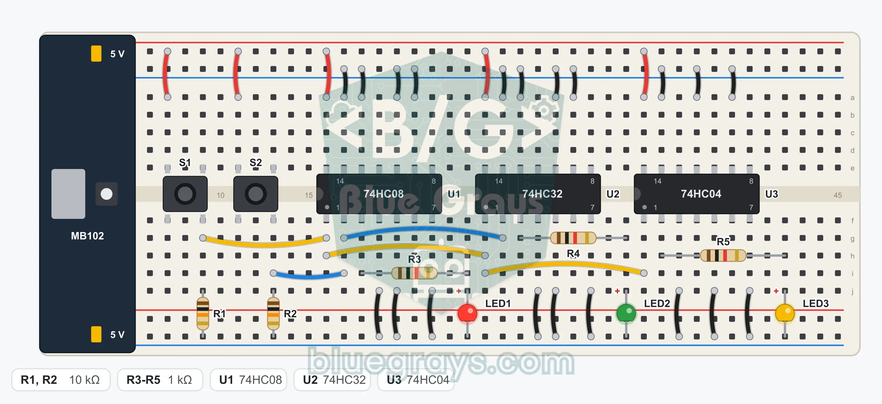
Plug the MB102 power module onto the end of the breadboard and set both jumper caps to the 5 V position. Leave the module's switch off for now.
- 2
Place the three ICs side by side over the center gap with their notches facing left: from left to right 74HC08 (U1), 74HC32 (U2), 74HC04 (U3). Leave a gap of at least two rows between them. On all of them the bottom left corner is pin 1; the bottom row runs from 1 to 7, and the top row runs from 8 to 14 from right to left.
- 3
Connect pin 14 of all three ICs to the + rail with one jumper wire each.
- 4
Connect pin 7 of all three ICs to the GND (−) rail with one jumper wire each.
- 5
Tie off the unused inputs of U1: connect pins 4, 5, 9, 10, 12 and 13 to the GND rail with one jumper wire each. Pins 6, 8 and 11 stay unconnected.
- 6
Do the same on U2: pins 4, 5, 9, 10, 12 and 13 go to the GND rail. Pins 6, 8 and 11 stay unconnected.
- 7
Tie off the unused inputs of U3: connect pins 3, 5, 9, 11 and 13 to the GND rail with one jumper wire each. Pins 4, 6, 8, 10 and 12 stay unconnected.
- 8
Place the S1 button (A) over the center gap; connect the leg at one corner to the + rail with a jumper wire. The row of the leg at the diagonally opposite corner is the A line; fit R1 (10 kΩ) between this row and the GND rail.
- 9
Place the S2 button (B) the same way; connect the leg at one corner to the + rail. The row of the leg at the diagonally opposite corner is the B line; fit R2 (10 kΩ) between this row and the GND rail.
- 10
Run one jumper wire from the A line to U1 pin 1, one from there to U2 pin 1, and one from there to U3 pin 1. This way A reaches all three ICs at once.
- 11
Run one jumper wire from the B line to U1 pin 2 and one from there to U2 pin 2.
- 12
Fit R3 (1 kΩ) from the row of U1 pin 3 to an empty row. Plug the long leg of LED1 (red) into that row and its short leg into the GND rail. This LED is the AND output.
- 13
Fit R4 (1 kΩ) from the row of U2 pin 3 to an empty row. Plug the long leg of LED2 (green) into that row and its short leg into the GND rail. This LED is the OR output.
- 14
Fit R5 (1 kΩ) from the row of U3 pin 2 to an empty row. Plug the long leg of LED3 (yellow) into that row and its short leg into the GND rail. This LED is the NOT output.
- 15
Compare the connections with the schematic, then switch on the power module.
Petua: biarkan bateri atau bekalan kuasa tidak disambung semasa membuat pendawaian.
Langkah Ujian
- 1
Switch on the power module and do not touch the buttons: only the yellow LED must light.
- 2
Press only S1 (A): green lights, yellow goes out, red stays off.
- 3
Press only S2 (B): green lights, yellow stays on, red stays off.
- 4
Press both buttons together: red and green light, yellow goes out.
- 5
Compare the four cases with the truth table row by row.
Cara Ia Berfungsi
Two buttons provide the A and B inputs; the 74HC08 does the AND operation, the 74HC32 the OR and the 74HC04 the NOT, and the results are shown on three LEDs.
Logic 0 and 1
Digital circuits have only two values: a voltage close to GND counts as 0, a voltage close to the supply counts as 1. When you are not pressing the button, the 10 kΩ resistor pulls the input to GND and the input is 0. When you press it, the input is connected to the + rail and becomes 1.
AND: both together
The output of the AND gate is 1 only while both of its inputs are 1. Think of two switches in series: current flows only when both are closed. That is why the red LED lights only when you press both buttons together.
OR: at least one
The output of the OR gate is 1 while at least one of its inputs is 1. It is like two switches in parallel: if either one is closed, current flows. The green LED lights when you press one of the buttons or both at once.
NOT: invert
The NOT gate has a single input and its output is always the opposite of its input. The yellow LED lights when you are not pressing the A button and goes out when you press it. Because the B button is not connected to this gate, it does not affect the yellow LED.
Same input, three gates
The A line goes to all three ICs at once, the B line to the AND and OR ICs. Because CMOS inputs draw almost no current, a single button drives many gates without trouble. This way you see side by side how three different operations respond to the same inputs.
Jadual Kebenaran
| A (S1) | B (S2) | AND (red) | OR (green) | NOT A (yellow) |
|---|---|---|---|---|
| 0 | 0 | 0 | 0 | 1 |
| 0 | 1 | 0 | 1 | 1 |
| 1 | 0 | 0 | 1 | 0 |
| 1 | 1 | 1 | 1 | 0 |
While a button is pressed, its input is 1. While an output is 1, its LED lights.
Formula
AND operation
Y = A · B
Contoh: For A = 1, B = 0: Y = 1 · 0 = 0; the red LED is off
OR operation
Y = A + B
Contoh: For A = 1, B = 0: Y = 1 + 0 = 1; the green LED is on. In logic, 1 + 1 is also 1
NOT operation
Y = Ā
Contoh: For A = 0: Y = 1; the yellow LED is on
LED current
I = (Vout − VLED) / R3
Contoh: (5 V − 2 V) / 1 kΩ = 3 mA; below the 4 mA that is the safe limit for a 74HC output
Kesilapan Lazim
The red or green LED lights by itself.
R1 or R2 is missing. The A and B lines must be pulled to GND through 10 kΩ.
One IC does not respond at all.
Pin 14 of that IC is not connected to the + rail, or its pin 7 is not connected to GND. Each IC has its own supply connections.
The LEDs of AND and OR seem to have swapped places.
The 74HC08 and the 74HC32 have been swapped. Read the markings on top of the ICs.
The yellow LED is always on.
The A line does not reach U3 pin 1, or R5 is plugged into another pin instead of pin 2.
Soalan Lazim
Mengapakah LED kuning menyala walaupun saya tidak menekan butang?
LED kuning disambungkan ke get NOT, dan get NOT memberikan songsangan inputnya. Apabila kamu tidak menekan butang A, input ialah 0, output menjadi 1 dan LED menyala. Apabila kamu menekan A, input menjadi 1, output jatuh ke 0 dan LED padam. Jadi litar berfungsi tepat seperti yang dijangka.
Mengapakah ada lebih daripada satu get di dalam IC?
Dalam pakej 14 pin, tinggal 12 pin selepas dua pin diketepikan untuk bekalan. Get dua input menggunakan 3 pin, jadi 4 get muat di dalamnya; bagi get NOT satu input, 6 muat. Dalam litar ini, kita hanya menggunakan get pertama setiap IC.
Mengapakah saya menyambungkan input get yang tidak digunakan ke GND?
Jika input CMOS dibiarkan terapung, voltannya merayau antara 0 dan 1. Dalam keadaan itu, get menarik arus yang tidak perlu, boleh menjadi panas dan boleh mengganggu get jirannya. Menyambungkan input ke GND menahannya pada 0 yang stabil. Output pula tidak disambungkan ke mana-mana.
Apakah kegunaan get ini dalam kehidupan sebenar?
Setiap keputusan digital dibina daripada tiga operasi ini. Jika pintu tertutup DAN penggera diaktifkan, bunyikan siren; jika pintu depan ATAU pintu belakang telah dibuka, hidupkan lampu; jika di luar TIDAK gelap, matikan lampu. Pemproses juga berfungsi dengan menggabungkan berbilion get seperti ini.