
Basic Gates: AND, OR and NOT Circuit
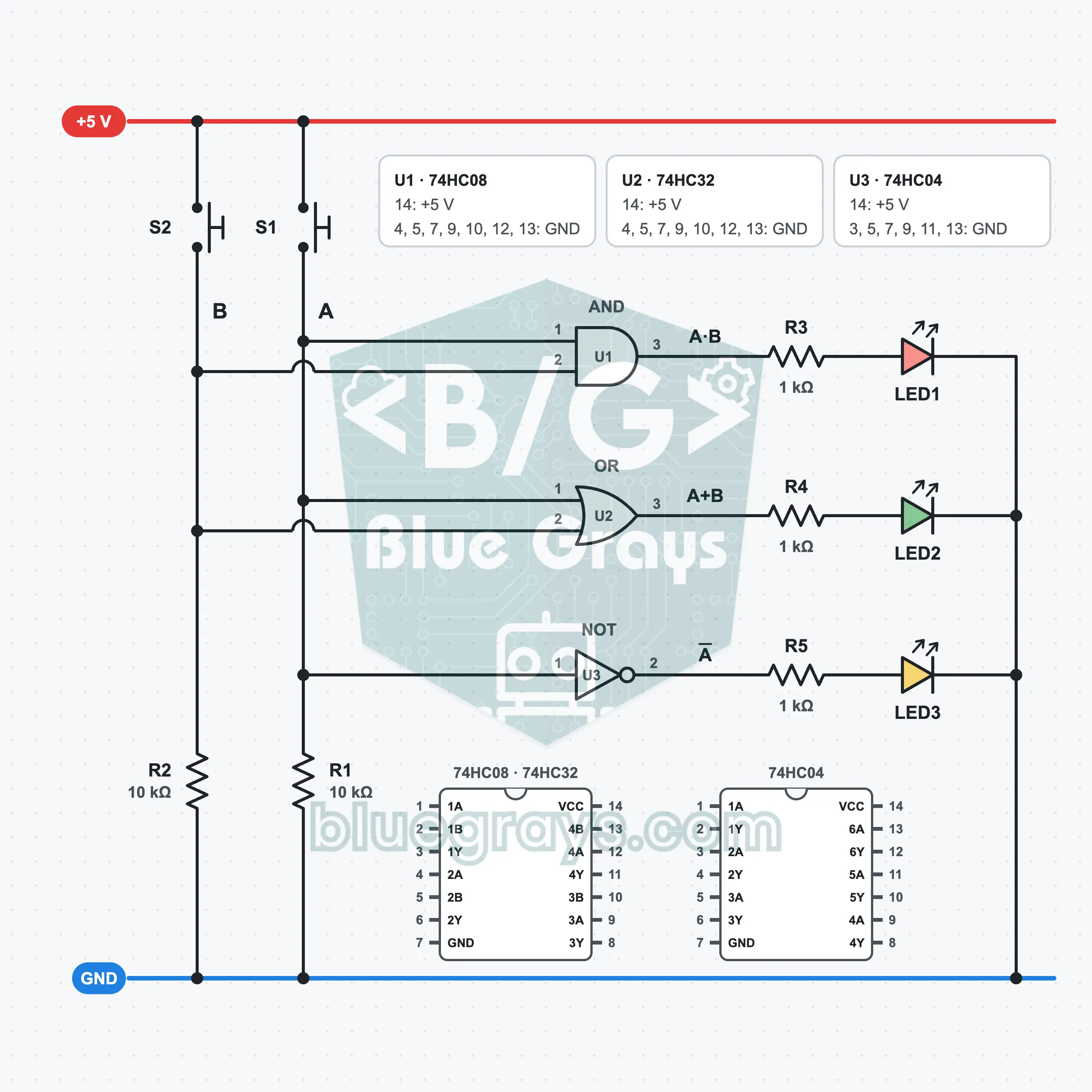
Try out the three building blocks of digital electronics on the same breadboard. Two buttons become your A and B inputs; the red LED shows the result of the AND gate, the green LED the OR gate and the yellow LED the NOT gate. With the 74HC08, 74HC32 and 74HC04 ICs you try the four button combinations one by one and work out the truth table with your own eyes.
Video
Circuit Diagram
Breadboard Layout
Build Steps
- 1
Plug the MB102 power module onto the end of the breadboard and set both jumper caps to the 5 V position. Leave the module's switch off for now.
- 2
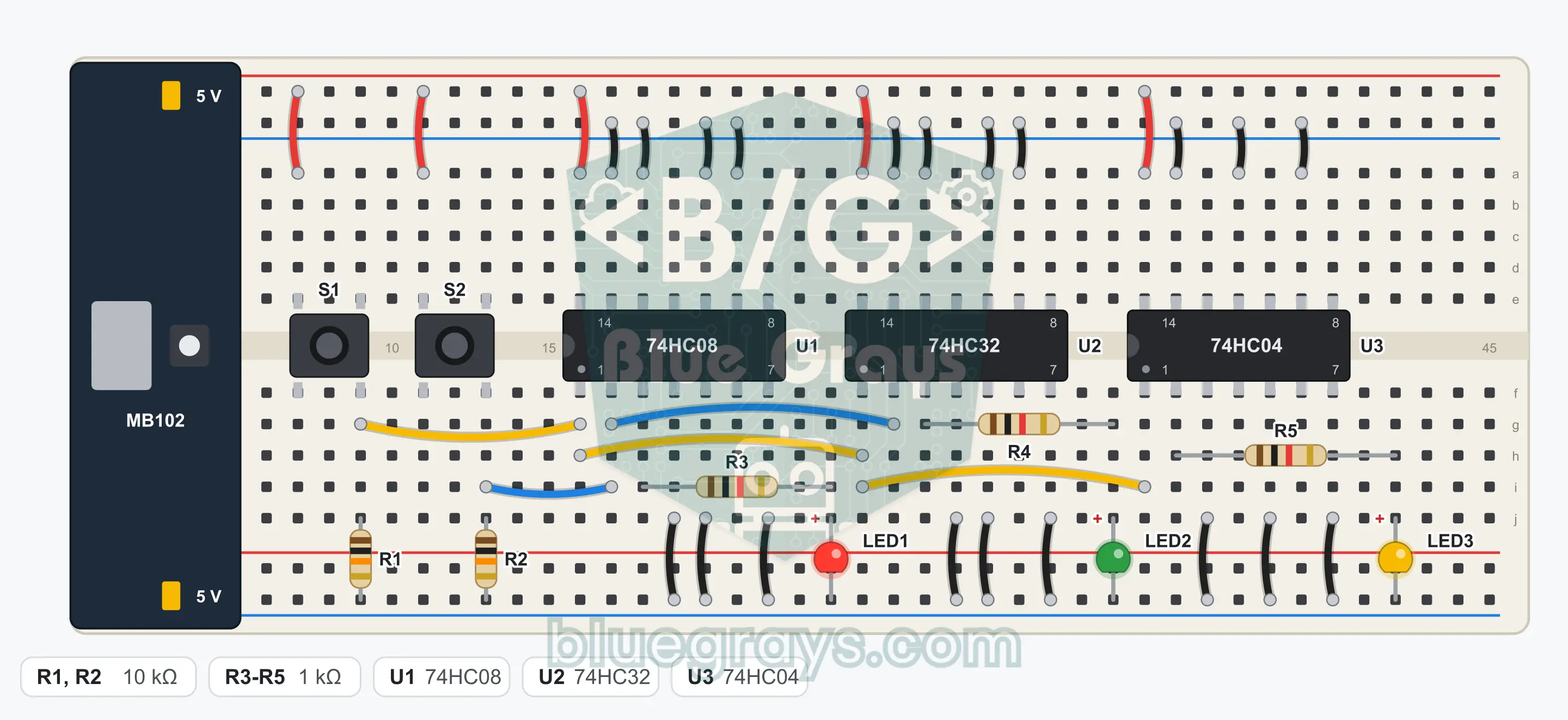
Place the three ICs side by side over the center gap with their notches facing left: from left to right 74HC08 (U1), 74HC32 (U2), 74HC04 (U3). Leave a gap of at least two rows between them. On all of them the bottom left corner is pin 1; the bottom row runs from 1 to 7, and the top row runs from 8 to 14 from right to left.
- 3
Connect pin 14 of all three ICs to the + rail with one jumper wire each.
- 4
Connect pin 7 of all three ICs to the GND (−) rail with one jumper wire each.
- 5
Tie off the unused inputs of U1: connect pins 4, 5, 9, 10, 12 and 13 to the GND rail with one jumper wire each. Pins 6, 8 and 11 stay unconnected.
- 6
Do the same on U2: pins 4, 5, 9, 10, 12 and 13 go to the GND rail. Pins 6, 8 and 11 stay unconnected.
- 7
Tie off the unused inputs of U3: connect pins 3, 5, 9, 11 and 13 to the GND rail with one jumper wire each. Pins 4, 6, 8, 10 and 12 stay unconnected.
- 8
Place the S1 button (A) over the center gap; connect the leg at one corner to the + rail with a jumper wire. The row of the leg at the diagonally opposite corner is the A line; fit R1 (10 kΩ) between this row and the GND rail.
- 9
Place the S2 button (B) the same way; connect the leg at one corner to the + rail. The row of the leg at the diagonally opposite corner is the B line; fit R2 (10 kΩ) between this row and the GND rail.
- 10
Run one jumper wire from the A line to U1 pin 1, one from there to U2 pin 1, and one from there to U3 pin 1. This way A reaches all three ICs at once.
- 11
Run one jumper wire from the B line to U1 pin 2 and one from there to U2 pin 2.
- 12
Fit R3 (1 kΩ) from the row of U1 pin 3 to an empty row. Plug the long leg of LED1 (red) into that row and its short leg into the GND rail. This LED is the AND output.
- 13
Fit R4 (1 kΩ) from the row of U2 pin 3 to an empty row. Plug the long leg of LED2 (green) into that row and its short leg into the GND rail. This LED is the OR output.
- 14
Fit R5 (1 kΩ) from the row of U3 pin 2 to an empty row. Plug the long leg of LED3 (yellow) into that row and its short leg into the GND rail. This LED is the NOT output.
- 15
Compare the connections with the schematic, then switch on the power module.
Tip: keep the battery or power supply disconnected while wiring.
Test Steps
- 1
Switch on the power module and do not touch the buttons: only the yellow LED must light.
- 2
Press only S1 (A): green lights, yellow goes out, red stays off.
- 3
Press only S2 (B): green lights, yellow stays on, red stays off.
- 4
Press both buttons together: red and green light, yellow goes out.
- 5
Compare the four cases with the truth table row by row.
How It Works
Two buttons provide the A and B inputs; the 74HC08 does the AND operation, the 74HC32 the OR and the 74HC04 the NOT, and the results are shown on three LEDs.
Logic 0 and 1
Digital circuits have only two values: a voltage close to GND counts as 0, a voltage close to the supply counts as 1. When you are not pressing the button, the 10 kΩ resistor pulls the input to GND and the input is 0. When you press it, the input is connected to the + rail and becomes 1.
AND: both together
The output of the AND gate is 1 only while both of its inputs are 1. Think of two switches in series: current flows only when both are closed. That is why the red LED lights only when you press both buttons together.
OR: at least one
The output of the OR gate is 1 while at least one of its inputs is 1. It is like two switches in parallel: if either one is closed, current flows. The green LED lights when you press one of the buttons or both at once.
NOT: invert
The NOT gate has a single input and its output is always the opposite of its input. The yellow LED lights when you are not pressing the A button and goes out when you press it. Because the B button is not connected to this gate, it does not affect the yellow LED.
Same input, three gates
The A line goes to all three ICs at once, the B line to the AND and OR ICs. Because CMOS inputs draw almost no current, a single button drives many gates without trouble. This way you see side by side how three different operations respond to the same inputs.
Truth Table
| A (S1) | B (S2) | AND (red) | OR (green) | NOT A (yellow) |
|---|---|---|---|---|
| 0 | 0 | 0 | 0 | 1 |
| 0 | 1 | 0 | 1 | 1 |
| 1 | 0 | 0 | 1 | 0 |
| 1 | 1 | 1 | 1 | 0 |
While a button is pressed, its input is 1. While an output is 1, its LED lights.
Formulas
AND operation
Y = A · B
Example: For A = 1, B = 0: Y = 1 · 0 = 0; the red LED is off
OR operation
Y = A + B
Example: For A = 1, B = 0: Y = 1 + 0 = 1; the green LED is on. In logic, 1 + 1 is also 1
NOT operation
Y = Ā
Example: For A = 0: Y = 1; the yellow LED is on
LED current
I = (Vout − VLED) / R3
Example: (5 V − 2 V) / 1 kΩ = 3 mA; below the 4 mA that is the safe limit for a 74HC output
Common Mistakes
The red or green LED lights by itself.
R1 or R2 is missing. The A and B lines must be pulled to GND through 10 kΩ.
One IC does not respond at all.
Pin 14 of that IC is not connected to the + rail, or its pin 7 is not connected to GND. Each IC has its own supply connections.
The LEDs of AND and OR seem to have swapped places.
The 74HC08 and the 74HC32 have been swapped. Read the markings on top of the ICs.
The yellow LED is always on.
The A line does not reach U3 pin 1, or R5 is plugged into another pin instead of pin 2.
FAQ
Why is the yellow LED lit even though I am not pressing the buttons?
The yellow LED is connected to the NOT gate, and a NOT gate gives the opposite of its input. When you are not pressing the A button the input is 0, the output becomes 1 and the LED lights. When you press A the input becomes 1, the output drops to 0 and the LED goes out. So the circuit is working exactly as expected.
Why is there more than one gate inside an IC?
In a 14-pin package, 12 pins are left after two pins are set aside for the supply. A two-input gate uses 3 pins, so 4 gates fit inside; of the single-input NOT gate, 6 fit. In this circuit we use only the first gate of each IC.
Why do I connect the inputs of the gates I am not using to GND?
If CMOS inputs are left floating, their voltage wanders between 0 and 1. In that case the gate draws unnecessary current, can heat up and can upset the neighboring gates. Connecting the inputs to GND holds them at a steady 0. The outputs, on the other hand, are not connected anywhere.
What are these gates good for in real life?
Every digital decision is built from these three operations. If the door is closed AND the alarm is armed, sound the siren; if the front door OR the back door has been opened, turn on the light; if it is NOT dark outside, turn off the lamp. Processors also work by bringing billions of gates like these together.