
Every Gate from NAND: One IC, Three Operations
Build the NAND, AND and NOT gates at the same time with a single 74HC00 IC. The NAND gate is universal: with enough NANDs, every logic circuit can be made. Two buttons become your inputs; the red LED shows the NAND result, the green LED the AND result and the yellow LED the NOT result. In the task you also get an OR gate out of the same IC.
Video
Circuit Diagram
Breadboard Layout
Build Steps
- 1
Plug the MB102 power module onto the end of the breadboard and set both jumper caps to the 5 V position. Leave the module's switch off for now.
- 2
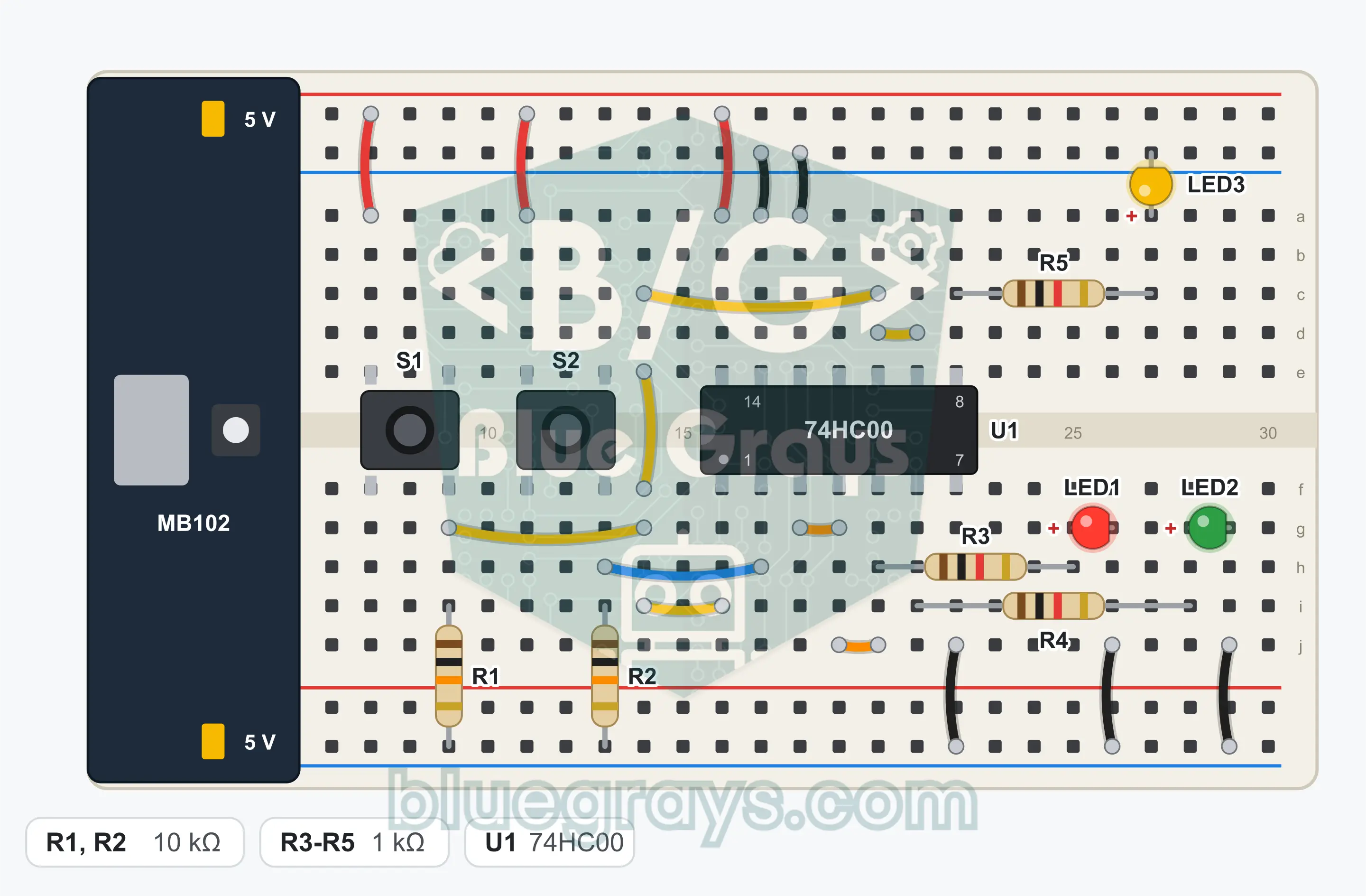
Place the 74HC00 (U1) over the center gap with its notch facing left. The bottom left corner is pin 1; the bottom row runs from 1 to 7 from left to right, and the top row runs from 8 to 14 from right to left.
- 3
Connect pin 14 to the + rail with a jumper wire and pin 7 to the GND (−) rail with a jumper wire.
- 4
The fourth gate is not used: connect pin 12 and pin 13 to the GND rail with one jumper wire each. Pin 11 stays unconnected.
- 5
Fit R1 (10 kΩ) between pin 1 and the GND rail.
- 6
Place the S1 button (A) over the center gap; connect the leg at one corner to the + rail with a jumper wire and the leg at the diagonally opposite corner to pin 1.
- 7
Fit R2 (10 kΩ) between pin 2 and the GND rail.
- 8
Place the S2 button (B) over the center gap; connect the leg at one corner to the + rail with a jumper wire and the leg at the diagonally opposite corner to pin 2.
- 9
Turn the second gate into an inverter: connect pin 3 to pin 4 with a jumper wire and pin 4 to pin 5 with a jumper wire.
- 10
Connect the third gate to A: connect pin 1 to pin 9 with a jumper wire and pin 9 to pin 10 with a jumper wire.
- 11
Fit R3 (1 kΩ) from the row of pin 3 to an empty row. Plug the long leg of LED1 (red) into that row and its short leg into the GND rail. This LED is the NAND output.
- 12
Fit R4 (1 kΩ) from the row of pin 6 to an empty row. Plug the long leg of LED2 (green) into that row and its short leg into the GND rail. This LED is the AND output.
- 13
Fit R5 (1 kΩ) from the row of pin 8 to an empty row. Plug the long leg of LED3 (yellow) into that row and its short leg into the GND rail. This LED is the NOT A output.
- 14
Compare the connections with the schematic, then switch on the power module.
Tip: keep the battery or power supply disconnected while wiring.
Test Steps
- 1
Switch on the power module and do not touch the buttons: the red and yellow LEDs must light, and the green one must be off.
- 2
Press only S1 (A): yellow goes out, red stays on, green stays off.
- 3
Press only S2 (B): nothing changes; red and yellow on, green off.
- 4
Press both buttons together: red goes out, green lights, yellow goes out.
- 5
Compare the four cases with the truth table: red and green must never light at the same time.
How It Works
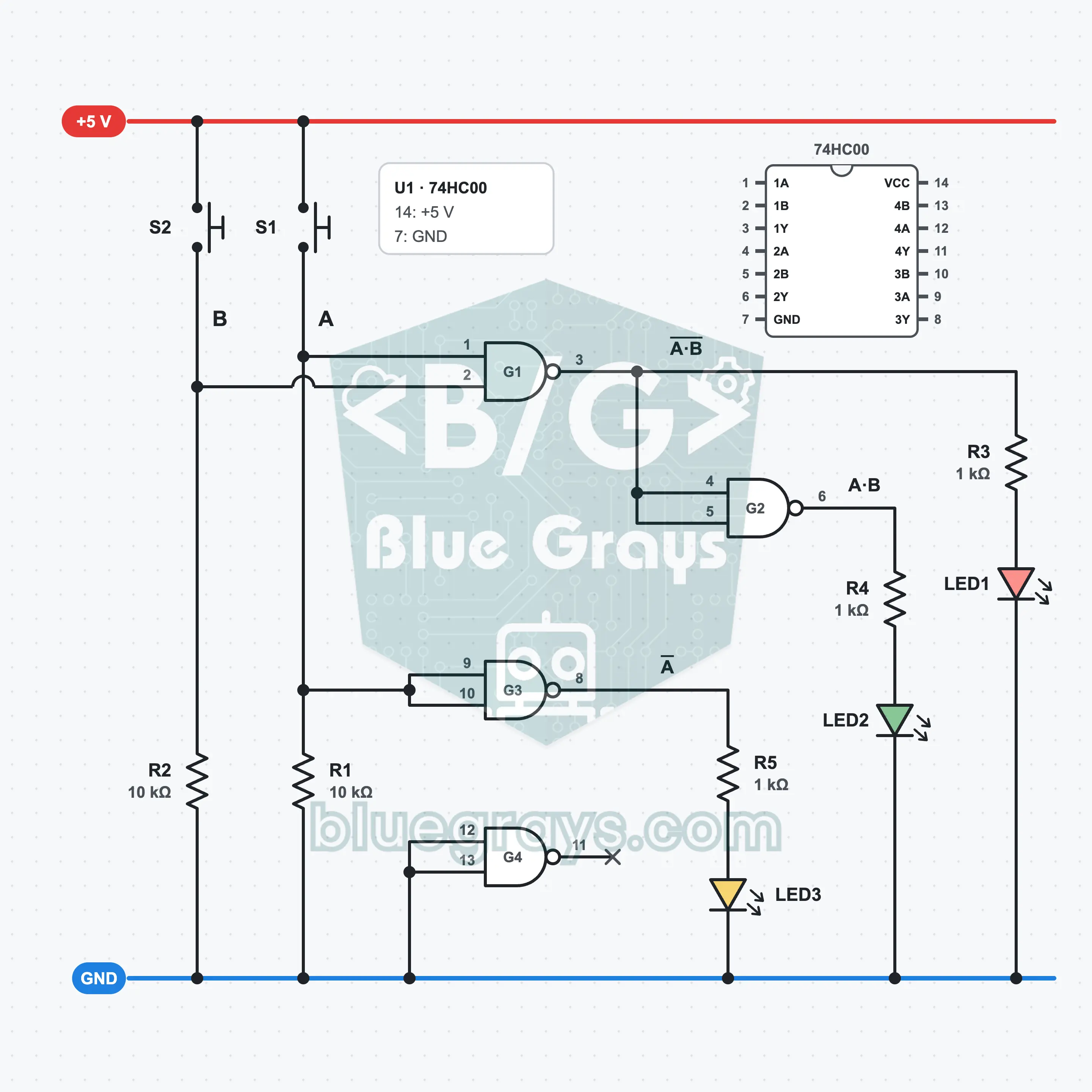
The first gate of the 74HC00 gives NAND; the second gate, with its inputs joined, turns it into AND, and the third gate produces the inverse of A. The three results appear on three LEDs.
NAND: the inverse of AND
The output of the NAND gate is 0 only while both of its inputs are 1; in the other three cases it is 1. Its name is a blend of the words NOT and AND. The first gate (pins 1 and 2 are the inputs, pin 3 the output) gives the NAND of the A and B buttons and drives the red LED.
Making NOT from NAND
If you connect the two inputs of a NAND gate to each other, the inputs always take the same value. If both are 0 the output is 1, if both are 1 the output is 0. You now have an inverter. The third gate (pins 9 and 10 are the inputs, pin 8 the output) is wired this way and shows the inverse of A on the yellow LED.
Making AND from NAND
Since NAND is already the inverse of AND, if you invert it once more you get AND back. The second gate (pins 4 and 5 are the inputs, pin 6 the output) is wired as an inverter and flips the output of the first gate. That is why the green LED is always the exact opposite of the red one.
Universal gate
You were able to build NOT and AND from NAND. OR can be built too: inverting the inputs first and then passing them through a NAND is enough. With these three in hand you can make any logic circuit. That is why the NAND gate is called a universal gate, and the inside of many chips consists almost entirely of NANDs.
Truth Table
| A (S1) | B (S2) | NAND (red) | AND (green) | NOT A (yellow) |
|---|---|---|---|---|
| 0 | 0 | 1 | 0 | 1 |
| 0 | 1 | 1 | 0 | 1 |
| 1 | 0 | 1 | 0 | 0 |
| 1 | 1 | 0 | 1 | 0 |
While a button is pressed, its input is 1. NAND is read from pin 3, AND from pin 6 and NOT A from pin 8.
Formulas
NAND operation
Y = NOT (A · B)
Example: For A = 1, B = 1: A · B = 1, its inverse is 0; the red LED goes out
NOT from NAND
NAND(A, A) = NOT A
Example: For A = 0: NAND(0, 0) = 1; for A = 1: NAND(1, 1) = 0
AND from NAND
A · B = NOT (NAND(A, B))
Example: For A = 1, B = 1: NAND = 0, its inverse is 1; the green LED lights
OR from NAND (De Morgan's law)
A + B = NAND(NOT A, NOT B)
Example: For A = 1, B = 0: NAND(0, 1) = 1; for A = 0, B = 0: NAND(1, 1) = 0
LED current
I = (Vout − VLED) / R3
Example: (5 V − 2 V) / 1 kΩ = 3 mA; below the 4 mA that is the safe limit for a 74HC output
Common Mistakes
The green LED does not light at all.
Pins 3, 4 and 5 must be connected to each other. One of the two short jumper wires is missing.
The yellow LED does not go out when I press A.
Pin 9 and pin 10 must both be connected to the A line, that is, to pin 1. R5 goes into the row of pin 8.
The LEDs are unstable and change by themselves.
R1 or R2 is missing, or pins 12 and 13 are not connected to GND.
Red and green light at the same time.
R4 may be plugged into the row of pin 3 instead of pin 6. Count the pins again from the left.
FAQ
Why is the NAND gate called a universal gate?
Because using NAND gates alone you can build NOT, AND, OR and every other logic operation. Thanks to this, producing a single type of gate at the factory is enough. The NOR gate has the same property. AND or OR alone is not universal, because you cannot invert with them.
Why does NAND become a NOT gate when its two inputs are joined?
The NAND gate gives 0 while both of its inputs are 1, and 1 in the other cases. If you join the inputs, both always take the same value: if both are 0 the output is 1, if both are 1 the output is 0. So the output is always the opposite of the input, and that is the definition of the NOT gate.
Why are two LEDs lit without pressing the buttons?
When you are not pressing the buttons, A and B are 0. The NAND gate gives 0 only while both inputs are 1, so right now its output is 1 and the red LED lights. The yellow LED shows the inverse of A; because A is 0, it lights too. The green AND LED is off.
Can I use a 7400 or 74LS00 instead of the 74HC00?
The pin layouts are the same, but this circuit was designed for the 74HC00. In the old TTL families a floating input behaves like a 1; the 10 kΩ pull-down resistor cannot bring the input down to 0, and the outputs cannot deliver enough current to light the LED with this connection. The 74HCT00, on the other hand, works without any changes.