
SR Latch: 1-Bit Memory with Two NOR Gates
Cross-couple two NOR gates and you have a 1-bit memory. This SR latch, which you build with a 74HC02, sets the Q output to 1 when you press the S button, sets it to 0 when you press the R button, and keeps the last state when you release the button. This small structure is inside every flip-flop. You read the truth table off the LEDs and try out the forbidden state yourself too.
Video
Circuit Diagram
Breadboard Layout
Build Steps
- 1
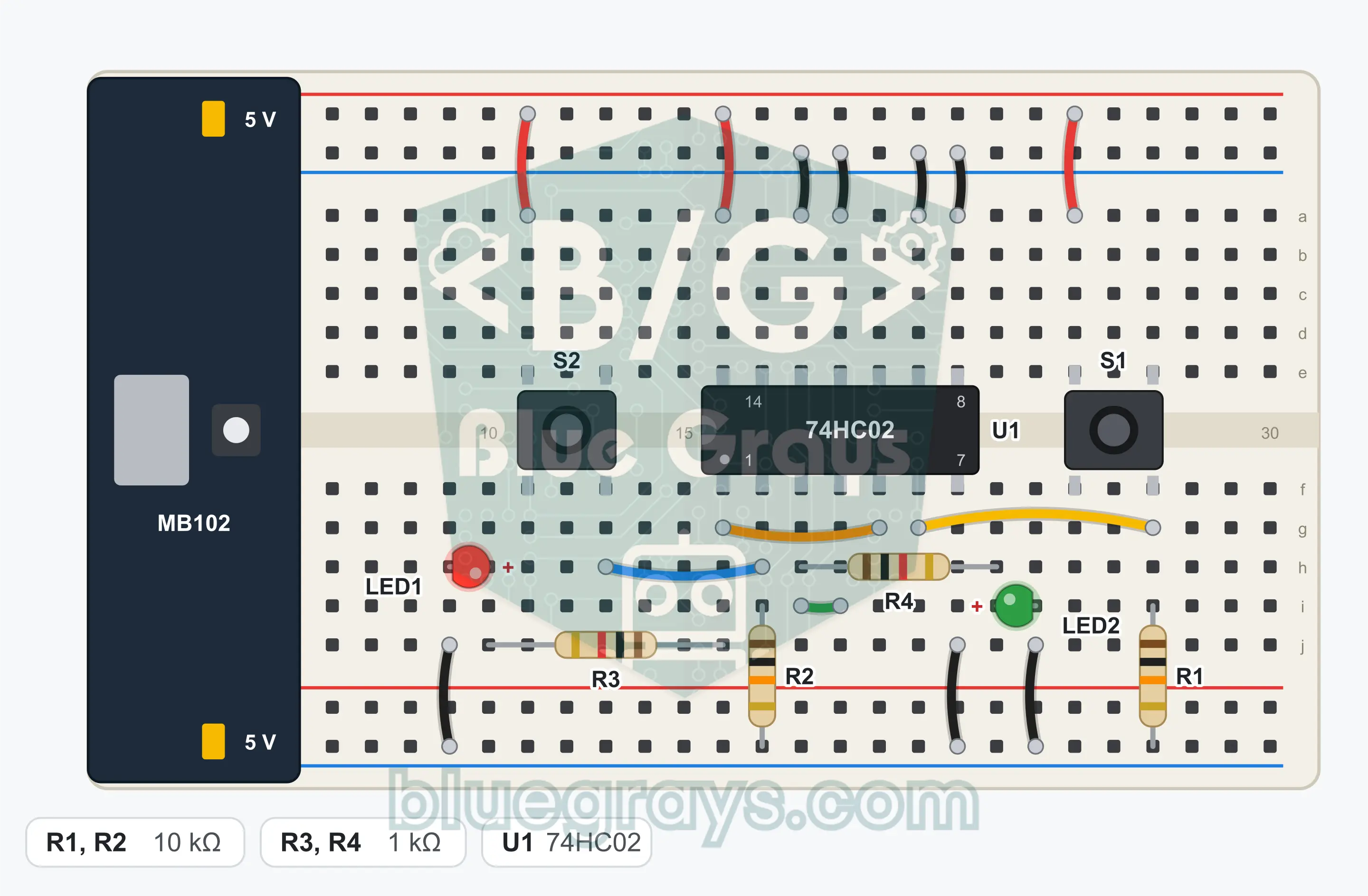
Plug the MB102 power module onto the end of the breadboard and set both jumper caps to the 5 V position. Leave the module's switch off for now.
- 2
Place the 74HC02 (U1) over the center gap with its notch facing left. The bottom left corner is pin 1; the bottom row runs from 1 to 7 from left to right, and the top row runs from 8 to 14 from right to left.
- 3
Connect pin 14 to the + rail with a jumper wire.
- 4
Connect pin 7 to the GND (−) rail with a jumper wire.
- 5
Tie off the unused inputs: connect pins 8, 9, 11 and 12 to the GND rail with one short jumper wire each. Pins 10 and 13 stay unconnected.
- 6
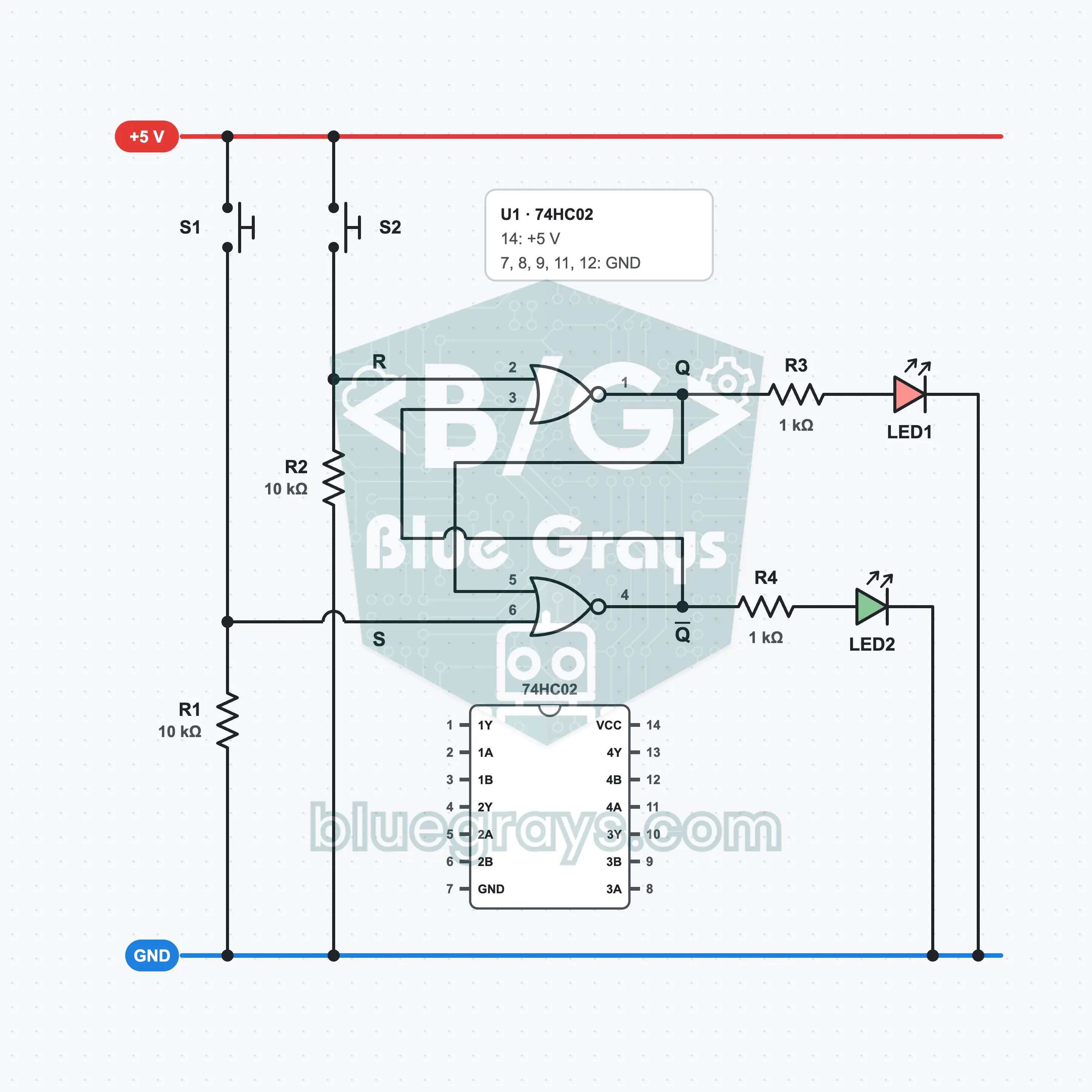
Connect pin 1 (Q) to pin 5 with a jumper wire.
- 7
Connect pin 4 (Q̄) to pin 3 with a jumper wire.
- 8
Fit R1 (10 kΩ) between pin 6 and the GND rail.
- 9
Fit R2 (10 kΩ) between pin 2 and the GND rail.
- 10
Place the S1 button over the center gap; connect the leg at one corner to the + rail with a jumper wire and the leg at the diagonally opposite corner to pin 6.
- 11
Place the S2 button over the center gap; connect the leg at one corner to the + rail with a jumper wire and the leg at the diagonally opposite corner to pin 2.
- 12
Fit R3 (1 kΩ): one end into the row of pin 1, the other end into an empty row.
- 13
Fit LED1 (red): long leg (anode) into the row of R3's free end, short leg (cathode) into the GND rail.
- 14
Fit R4 (1 kΩ): one end into the row of pin 4, the other end into an empty row.
- 15
Fit LED2 (green): long leg (anode) into the row of R4's free end, short leg (cathode) into the GND rail.
- 16
Compare the connections with the schematic, then switch on the power module.
Tip: keep the battery or power supply disconnected while wiring.
Test Steps
- 1
Switch on the power module: only one of the LEDs must light. Which one lights at power-on is not predictable.
- 2
Press S1 (S) once briefly: the red LED must light and the green one must go out. The state must not change when you release the button.
- 3
Press S2 (R) once briefly: red must go out, green must light and stay that way.
- 4
Press both buttons together: both LEDs go out. This is the forbidden state.
- 5
Try the four rows of the truth table one by one and compare them with the LEDs.
How It Works
When the two NOR gates of the 74HC02 are cross-coupled, they become an SR latch: S1 sets the Q output to 1, S2 sets it to 0, and the circuit keeps the last state.
What does a NOR gate do?
The output of a NOR gate is 1 only while both of its inputs are 0. If either input becomes 1, the output drops to 0. So a single 1 is enough to silence the gate. The whole behavior of the latch follows from this rule.
Cross-coupling
The upper gate produces the Q output and the lower gate the Q̄ output. One input of each gate is connected to a button, and the other input to the output of the opposite gate. This way each output affects the other, and the circuit feeds its own state.
S: set
When you press S1, pin 6 goes high and Q̄, the output of the lower gate, drops to 0. Both inputs of the upper gate are now 0 (R = 0, Q̄ = 0), so Q becomes 1. Q being 1 keeps silencing the lower gate; the state is kept even if you release the button.
R: reset
When you press S2, pin 2 goes high and Q drops to 0. Because both inputs of the lower gate stay at 0, Q̄ becomes 1, and this time it silences the upper gate. The circuit latches in the new state.
Forbidden state
If S and R are 1 together, both gates are silenced: Q = 0 and Q̄ = 0. The outputs are no longer the inverse of each other. If you release the buttons at the same moment, there is no telling which gate will recover first; that is why this input combination is avoided.
Truth Table
| S (S1) | R (S2) | Q (red) | Q̄ (green) |
|---|---|---|---|
| 0 | 0 | Previous state | Previous state |
| 1 | 0 | 1 | 0 |
| 0 | 1 | 0 | 1 |
| 1 | 1 | 0 | 0 |
While a button is pressed, its input is 1. The last row is the forbidden state: both outputs become 0.
Formulas
Logic of the latch
Q = NOR(R, Q̄), Q̄ = NOR(S, Q)
Example: For S = 1, R = 0: Q̄ = NOR(1, Q) = 0 and Q = NOR(0, 0) = 1
LED current
I = (Vout − VLED) / R3
Example: (5 V − 2 V) / 1 kΩ = 3 mA; below the 4 mA that is the safe limit for a 74HC output
Current through the pull-down resistor while the button is pressed
I = Vcc / R1
Example: 5 V / 10 kΩ = 0.5 mA
Common Mistakes
The LED goes back to its old state when I release the button.
One of the cross jumper wires is missing. Pin 1 connects to pin 5, and pin 4 to pin 3.
The LEDs change by themselves.
R1 or R2 is not in place. Pin 6 and pin 2 must be pulled to GND through 10 kΩ; pins 8, 9, 11 and 12 also go to GND.
The IC heats up and nothing works.
Switch off the power. The IC may be fitted backwards: the notch must be on the left, pin 14 in the + rail and pin 7 at GND.
The outputs are the opposite of what I expected.
On the 74HC02 the outputs are pins 1 and 4, not pins 3 and 6. Count the connections again against the pinout.
FAQ
What is the difference between a latch and a flip-flop?
A latch responds the moment its input changes; it does not wait for a clock signal. A flip-flop, on the other hand, looks at its input only on the edge of the clock pulse. There are latches inside flip-flops too; this circuit is their building block. In everyday language you will also see both of them called flip-flops.
Why do I connect the unused pins to GND?
There are four gates inside the 74HC02, and we use two of them. If CMOS inputs are left floating, their voltage wanders somewhere in the middle; the gate draws unnecessary current and its output can change by itself. Connecting the unused inputs to GND prevents this. The unused outputs, on the other hand, are left open.
Can I run this circuit from a 9 V battery?
No. The 74HC family works between 2 V and 6 V; 9 V destroys the IC. Use a 5 V power module or three AA batteries (4.5 V). Logic circuits that run from a 9 V battery need CD4000 series ICs; their NOR equivalent is the CD4001.
Will the IC be damaged if I press S and R at the same time?
It will not. Both outputs become 0 and both LEDs go out. The reason it is called the forbidden state is logical: Q and Q̄ are no longer the inverse of each other, and if you release the buttons at the same moment, there is no telling which state it will stay in. It does no electrical harm.