
D Flip-Flop: 1-Bit Memory with the 74HC74
Build the smallest piece of computer memory yourself. The D flip-flop inside the 74HC74 takes the value on its D input the moment a clock pulse arrives and keeps it until the next pulse. You give the data with a button and the clock pulse with a slide switch; the red LED shows what is inside the memory. You see the rising edge concept with your own eyes.
Video
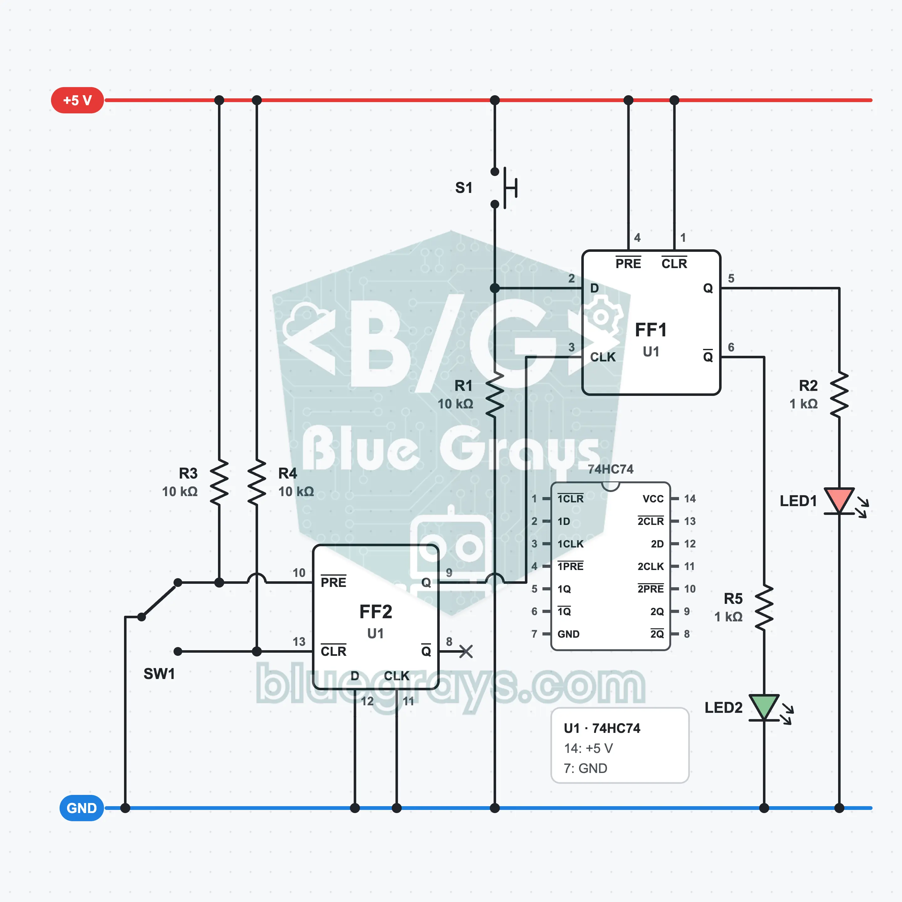
Circuit Diagram
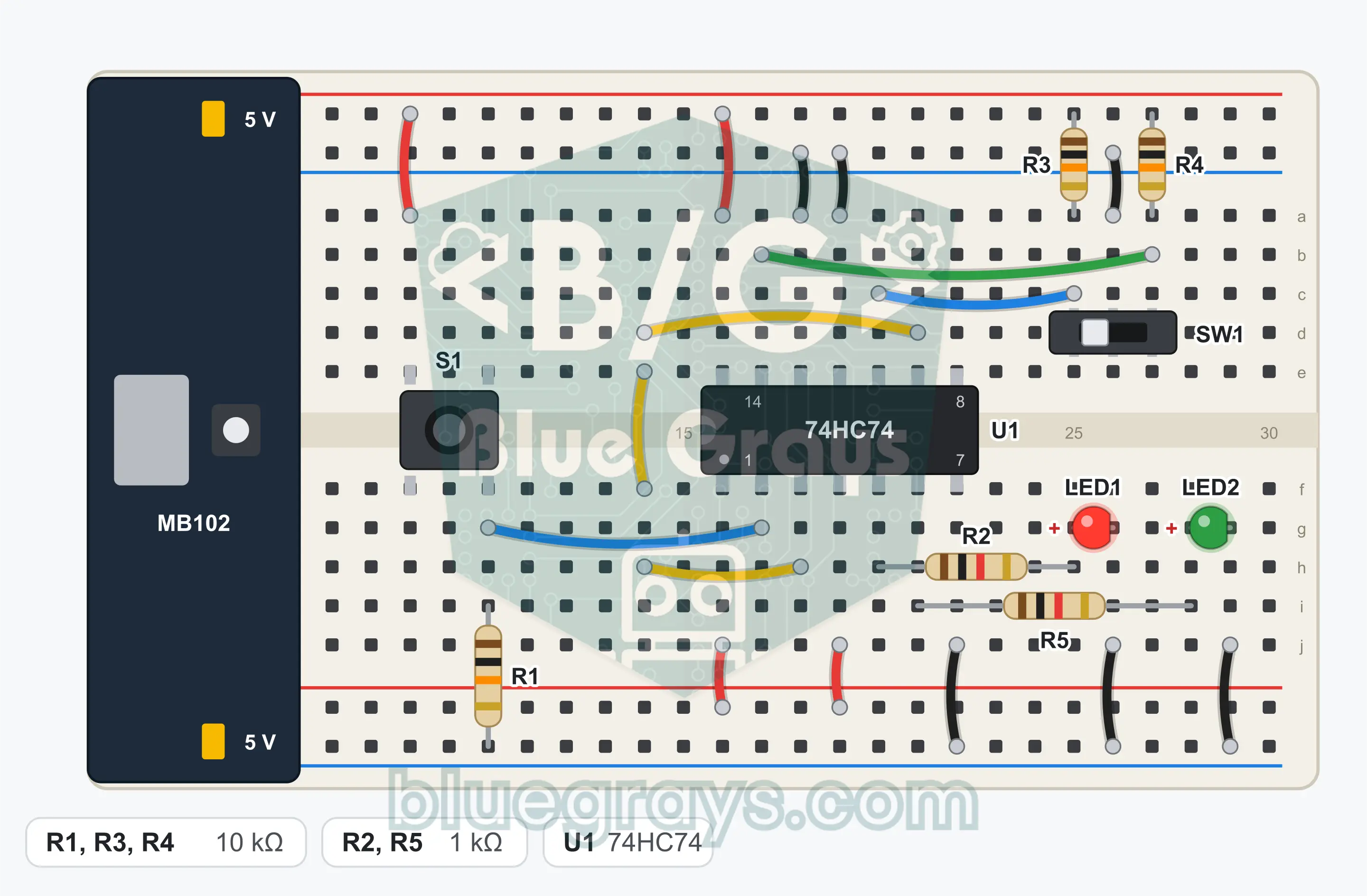
Breadboard Layout
Build Steps
- 1
Plug the MB102 power module onto the end of the breadboard and set both jumper caps to the 5 V position. Leave the module's switch off for now.
- 2
Place the 74HC74 (U1) over the center gap with its notch facing left. The bottom left corner is pin 1; the bottom row runs from 1 to 7 from left to right, and the top row runs from 8 to 14 from right to left.
- 3
Connect pin 14 to the + rail with a jumper wire and pin 7 to the GND (−) rail with a jumper wire.
- 4
Connect pin 4 and pin 1 to the + rail with one jumper wire each. These are the set and reset inputs of the first flip-flop; while they are in the + rail they are disabled.
- 5
Connect pin 12 and pin 11 to the GND rail with one jumper wire each.
- 6
Connect pin 9 to pin 3 with a jumper wire. The clock pulse travels through this wire.
- 7
Plug in the slide switch (SW1) so that its three legs sit in three separate rows. Connect its middle leg to the GND rail with a jumper wire.
- 8
Connect one outer leg of SW1 to pin 10 with a jumper wire. Fit R3 (10 kΩ) between pin 10 and the + rail. Let's call this side of the switch the 1 position.
- 9
Connect the other outer leg of SW1 to pin 13 with a jumper wire. Fit R4 (10 kΩ) between pin 13 and the + rail. This side is the 0 position.
- 10
Fit R1 (10 kΩ) between pin 2 and the GND rail.
- 11
Place the S1 button over the center gap; connect the leg at one corner to the + rail with a jumper wire and the leg at the diagonally opposite corner to pin 2.
- 12
Fit R2 (1 kΩ): one end into the row of pin 5, the other end into an empty row.
- 13
Fit LED1 (red): long leg (anode) into the row of R2's free end, short leg (cathode) into the GND rail.
- 14
Fit R5 (1 kΩ): one end into the row of pin 6, the other end into an empty row.
- 15
Fit LED2 (green): long leg (anode) into the row of R5's free end, short leg (cathode) into the GND rail. Pin 8 stays unconnected.
- 16
Compare the connections with the schematic, move SW1 to the 0 position, then switch on the power module.
Tip: keep the battery or power supply disconnected while wiring.
Test Steps
- 1
Switch on the power module: only one of the LEDs must light. Which one lights at power-on is not predictable.
- 2
Hold S1 down and slide SW1 to the 1 position: the red LED must light and the green one must go out. The memory has written a 1.
- 3
Release S1 and move SW1 back to the 0 position: nothing must change. The memory is keeping the 1.
- 4
Without pressing S1, slide SW1 to the 1 position again: red goes out, green lights. This time the memory has written a 0.
- 5
Without touching SW1, press and release S1 a few times: the LEDs must not change. Without a clock pulse the D input is not read.
How It Works
The D flip-flop of the 74HC74 copies the value on D to Q the moment the clock input rises from 0 to 1 and keeps it until the next pulse. S1 gives the data, SW1 the clock pulse.
The D input and the clock
The D flip-flop has two important inputs: D, the data to be stored, and the clock (CLK), which says when to store it. The flip-flop does not watch D all the time; it looks once, only when a clock pulse arrives, and puts the value it sees on the Q output.
Rising edge
The 74HC74 looks at the D input the moment the clock signal rises from 0 to 1. This moment is called the rising edge. While the clock sits at 1 or falls to 0, change D as much as you like; Q does not budge. It is like the shutter of a camera: only the picture at the moment you press remains.
Q and Q̄
Pin 5 (Q) gives the stored bit and pin 6 (Q̄) gives its inverse. Because the red LED is connected to Q and the green LED to Q̄, red lights while there is a 1 in the memory and green while there is a 0. The two LEDs never light at the same time.
A clean clock pulse
The set (pin 10) and reset (pin 13) inputs of the second flip-flop in the IC are active at 0. Because SW1 connects its middle terminal to GND, whichever side the switch touches, that input acts: in the 1 position pin 9 is high, in the 0 position it is low. Even if the switch bounces, the output settles at the first touch and produces a single clean edge.
The set and reset pins
The pin 4 (set) and pin 1 (reset) inputs of the first flip-flop can set Q directly to 1 or 0 without waiting for the clock. In this circuit we disabled both by connecting them to the + rail; this way Q changes only on the clock edge.
Truth Table
| Clock (SW1) | D (S1) | Q (red) | Q̄ (green) |
|---|---|---|---|
| 0 to 1 | 0 | 0 | 1 |
| 0 to 1 | 1 | 1 | 0 |
| Holding at 0 or 1 | Don't care | Previous state | Previous state |
| 1 to 0 | Don't care | Previous state | Previous state |
While S1 is pressed, D = 1. Q is updated only as the clock rises from 0 to 1.
Formulas
D flip-flop rule
On the rising edge: Q(new) = D
Example: If the clock rises from 0 to 1 while D = 1, Q becomes 1 and Q̄ becomes 0
Memory capacity
Number of states = 2^n (n: number of flip-flops)
Example: 1 flip-flop stores 2^1 = 2 states; 8 flip-flops side by side make 2^8 = 256 states, that is, 1 byte
LED current
I = (Vout − VLED) / R2
Example: (5 V − 2 V) / 1 kΩ = 3 mA; below the 4 mA that is the safe limit for a 74HC output
Common Mistakes
Nothing happens when I slide the switch.
The jumper wire between pin 9 and pin 3 is missing, or the middle leg of SW1 is not at GND.
The LED does not change right away when I press S1.
This is not a fault, it is the circuit itself. The D input is read only at the moment SW1 is slid to the 1 position.
The LEDs change at random.
R1 is not pulling pin 2 to GND, or one of pins 1, 4, 11, 12 has been left floating.
The IC heats up.
Switch off the power at once. The IC may be fitted backwards, or a voltage higher than 5 V may have been applied.
FAQ
Why do I give the clock pulse with a slide switch and not with a button?
The metal contacts inside a button bounce several times as you press and produce dozens of pulses in a single press. The flip-flop counts every one of them as a separate clock pulse. The slide switch, together with the second flip-flop in the IC, swallows this bounce and gives one clean pulse every time you slide it.
What does rising edge mean?
It is the moment the clock signal goes from 0 to 1. The 74HC74 looks at the D input only at this moment. While the clock is holding at 1, holding at 0 or falling from 1 to 0, the output does not change whatever D is. Thanks to this, all the memories in a circuit are updated at the same moment.
Is the memory erased when I switch off the power?
Yes. A flip-flop holds its information only while the supply is present; when you cut the power and switch it back on, it wakes up in a random state. The RAM in computers works the same way. For permanent storage, different memory types such as flash or EEPROM are used.
What is the second flip-flop in the IC for?
There are two independent D flip-flops inside the 74HC74. The first one works as the memory. We connect the set and reset pins of the second one to the slide switch and use it as a debouncer. This way we get a clean clock signal without buying an extra IC.