
JK Flip-Flop: Four-Mode Memory with the CD4027
The JK flip-flop is the most capable member of the flip-flop family: with a single IC you try all of the hold, set, reset and toggle modes and read the truth table off the LEDs. In the circuit you build with the CD4027, you pick the mode with the J and K buttons and give the clock pulse with a slide switch. The yellow LED shows the clock, and the red LED shows the memory.
Video
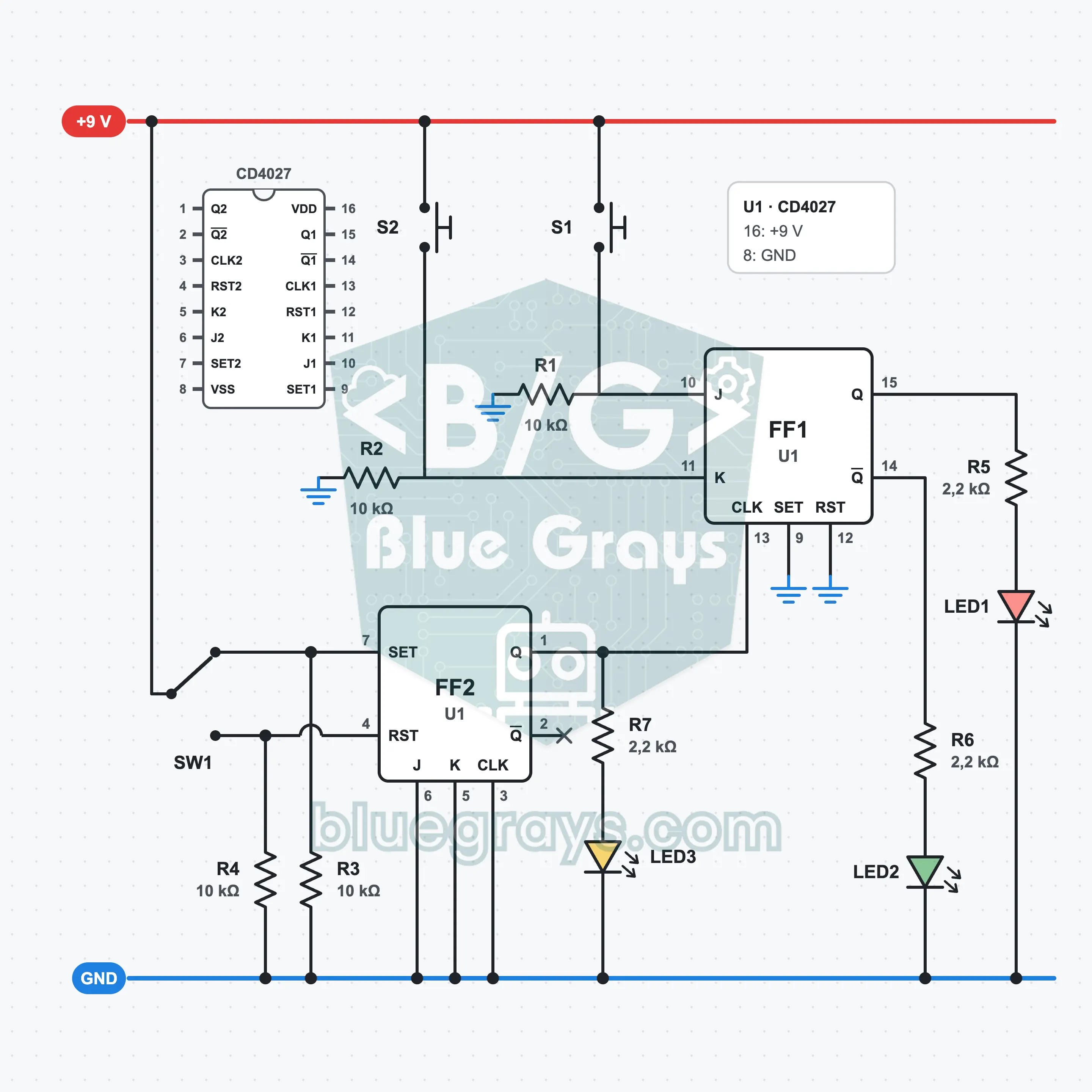
Circuit Diagram
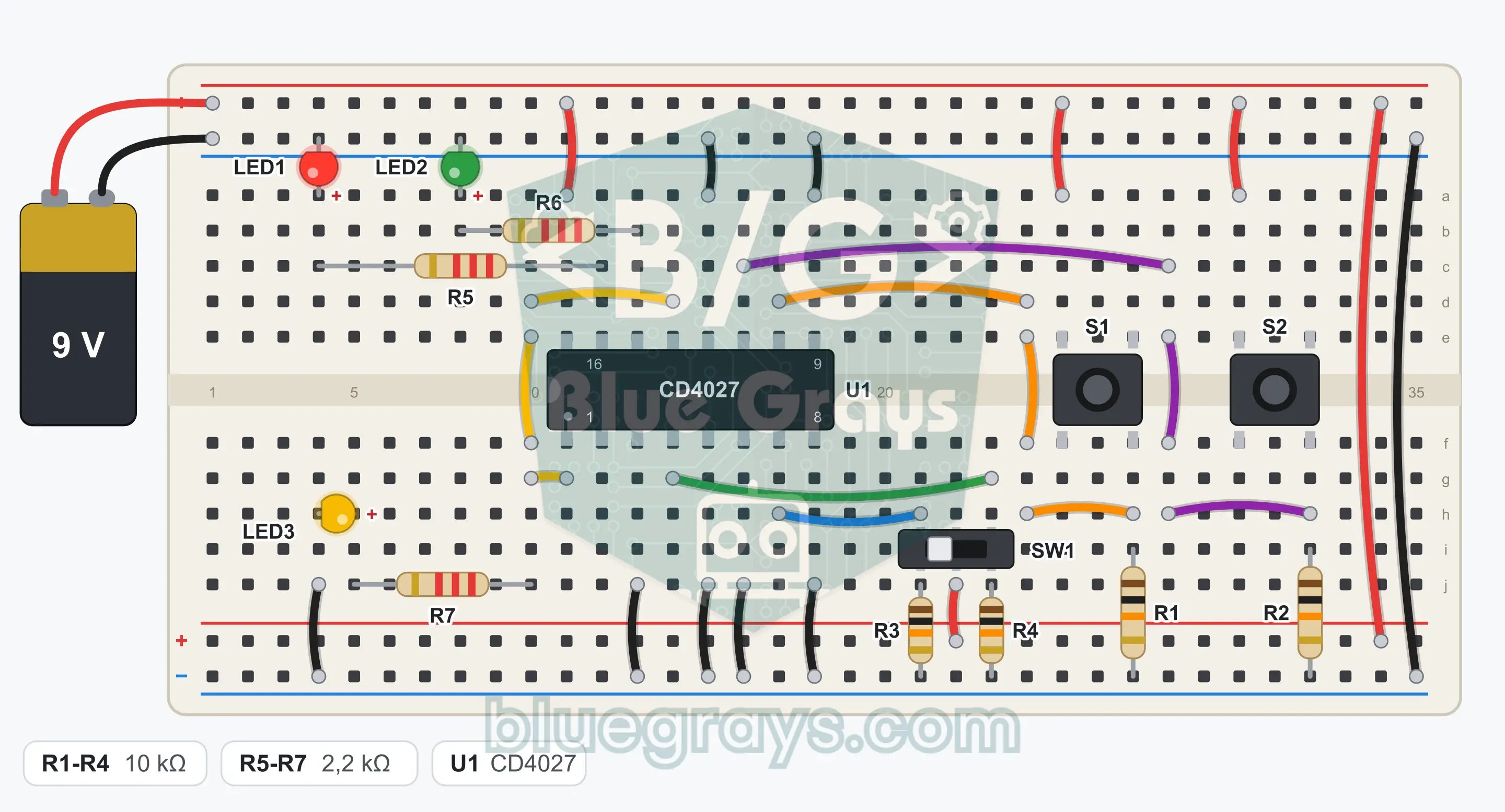
Breadboard Layout
Build Steps
- 1
Place the CD4027 (U1) over the center gap with its notch facing left. The bottom left corner is pin 1; the bottom row runs from 1 to 8 from left to right, and the top row runs from 9 to 16 from right to left.
- 2
Connect pin 16 to the + rail with a jumper wire and pin 8 to the GND (−) rail with a jumper wire.
- 3
Connect pin 9 and pin 12 to the GND rail with one jumper wire each. These are the set and reset inputs of the first flip-flop; while they are at GND they are disabled.
- 4
Connect pins 6, 5 and 3 to the GND rail with one jumper wire each. The J, K and clock inputs of the second flip-flop are not used.
- 5
Connect pin 1 to pin 13 with a jumper wire. The clock pulse travels through this wire.
- 6
Plug in the slide switch (SW1) so that its three legs sit in three separate rows. Connect its middle leg to the + rail with a jumper wire.
- 7
Connect one outer leg of SW1 to pin 7 with a jumper wire. Fit R3 (10 kΩ) between pin 7 and the GND rail. Let's call this side of the switch the 1 position.
- 8
Connect the other outer leg of SW1 to pin 4 with a jumper wire. Fit R4 (10 kΩ) between pin 4 and the GND rail. This side is the 0 position.
- 9
Fit R1 (10 kΩ) between pin 10 and the GND rail.
- 10
Place the S1 button (J) over the center gap; connect the leg at one corner to the + rail with a jumper wire and the leg at the diagonally opposite corner to pin 10.
- 11
Fit R2 (10 kΩ) between pin 11 and the GND rail.
- 12
Place the S2 button (K) over the center gap; connect the leg at one corner to the + rail with a jumper wire and the leg at the diagonally opposite corner to pin 11.
- 13
Fit R5 (2.2 kΩ) from the row of pin 15 to an empty row. Plug the long leg of LED1 (red) into that row and its short leg into the GND rail.
- 14
Fit R6 (2.2 kΩ) from the row of pin 14 to an empty row. Plug the long leg of LED2 (green) into that row and its short leg into the GND rail.
- 15
Fit R7 (2.2 kΩ) from the row of pin 1 to an empty row. Plug the long leg of LED3 (yellow) into that row and its short leg into the GND rail. Pin 2 stays unconnected.
- 16
Plug the red wire of the battery clip into the + rail and the black wire into the GND rail. Compare the connections with the schematic, move SW1 to the 0 position, then snap the battery onto the clip.
Tip: keep the battery or power supply disconnected while wiring.
Test Steps
- 1
Connect the battery: the yellow LED must be off, and only one of the red and green LEDs must light.
- 2
Hold S1 (J) down and slide SW1 to the 1 position: the yellow LED lights, the red LED lights. This is set mode.
- 3
Move SW1 to the 0 position. Hold S2 (K) down and slide SW1 to the 1 position again: red goes out, green lights. This is reset mode.
- 4
Without pressing any button, slide SW1 back and forth a few times: the yellow LED flashes, but red and green do not change. This is hold mode.
- 5
Hold both buttons down at once and slide SW1 back and forth: every time SW1 comes to the 1 position, red and green swap. This is toggle mode.
How It Works
The JK flip-flop of the CD4027 looks at the J and K inputs the moment the clock rises from 0 to 1: it holds, sets, resets or toggles the output. S1 gives J, S2 gives K and SW1 gives the clock pulse.
Two inputs, four modes
The J and K inputs tell the flip-flop what to do on the next clock pulse. If both are 0, the output stays as it is. If only J is 1, the output becomes 1. If only K is 1, the output becomes 0. If both are 1, the output flips to the opposite of its current state.
The moment of decision: the rising edge
The CD4027 looks at J and K only at the moment the clock input (pin 13) rises from 0 to 1. You have to press and hold the buttons beforehand and then give the clock pulse. While there is no clock pulse, press the buttons as much as you like; the output does not change.
Toggling
While J = 1 and K = 1, Q changes state on every rising edge: if it is 0 it becomes 1, if it is 1 it becomes 0. When the clock has gone back and forth twice, Q has gone back and forth once. So the frequency of the signal on Q is half that of the clock. Counters are built on this property.
A clean clock pulse
The set (pin 7) and reset (pin 4) inputs of the second flip-flop in the IC are active at 1. Because SW1 connects its middle terminal to the + rail, whichever side the switch touches, that input acts: in the 1 position pin 1 is high, in the 0 position it is low. Even if the switch bounces, the output settles at the first touch.
What is different about the CD4000 series
The CD4027 works over a wide supply range and connects directly to a 9 V battery. In return, its outputs are weak; that is why 2.2 kΩ was chosen for the LED resistors. The set and reset inputs are also active at 1, the opposite of the 74HC74, and are connected to GND when they are not used.
Truth Table
| J (S1) | K (S2) | Q after the clock pulse | Mode |
|---|---|---|---|
| 0 | 0 | Previous state | Hold |
| 1 | 0 | 1 | Set |
| 0 | 1 | 0 | Reset |
| 1 | 1 | Inverse of previous state | Toggle |
Q is updated only as the clock rises from 0 to 1 (as SW1 moves to the 1 position). Q̄ is always the inverse of Q.
Formulas
JK flip-flop equation
Q(new) = J × Q̄ + K̄ × Q
Example: For J = 1, K = 1, Q = 0: 1 × 1 + 0 × 0 = 1; the output has toggled
Output frequency in toggle mode
fQ = fclk / 2
Example: If you bring SW1 to the 1 position 2 times a second (2 Hz), the red LED lights 1 time a second (1 Hz)
LED current (upper limit)
I = (Vout − VLED) / R5
Example: (9 V − 2 V) / 2.2 kΩ ≈ 3.2 mA; because the CD4027 output drops a little under load, the real current is somewhat below this
Current through the pull-down resistor while the button is pressed
I = Vcc / R1
Example: 9 V / 10 kΩ = 0.9 mA
Common Mistakes
I press a button and the LED does not change.
This is normal. You have to slide SW1 to the 1 position while holding the button down; the inputs are read only on the clock edge.
The yellow LED does not light; there is no clock pulse.
The middle leg of SW1 must be in the + rail. R3 and R4 must pull pin 7 and pin 4 to GND.
The output is always the same, whatever the buttons do.
Pin 9 or pin 12 is not at GND. These inputs are active at 1, and they must not be left floating either.
When I press both buttons, the output seems to change at random.
In toggle mode the state changes on every pulse; slide SW1 slowly and all the way. If the jumper wire between pin 1 and pin 13 is loose, extra pulses can occur.
FAQ
How is a JK flip-flop different from an SR latch?
On an SR latch, giving a 1 to both inputs at once is forbidden, because the result is undefined. The JK flip-flop turns this case into a useful mode: while J = 1 and K = 1, the output toggles on every clock pulse. It also looks at its inputs only on the clock edge, so its behavior is much more predictable.
Why does this circuit run on 9 V while the 74HC circuits want 5 V?
The CD4027 belongs to the CD4000 series and works between 3 V and 15 V; a 9 V battery suits it perfectly. The 74HC family, on the other hand, can take 6 V at most. If you want to mix the two families in the same circuit, you have to supply all of them with 5 V. Never give 9 V to a 74HC IC.
Why are the LED resistors 2.2 kΩ?
A CD4027 output can deliver only a few milliamps. With 2.2 kΩ the LED current stays at about 3 mA; the LED is clearly visible and the output voltage does not drop much. A smaller resistor does not make the LED noticeably brighter; it only strains the output and can upset the level of the clock signal.
What is toggle mode good for?
While J and K are both 1, the output changes state on every clock pulse. So the signal at the output flashes at half the speed of the clock. This divide-by-two operation is the basis of counters: flip-flops connected one after another count in binary. Digital clocks get their one-second tick this way too.