
T Flip-Flop: Divide-by-Two Circuit with the 74HC74
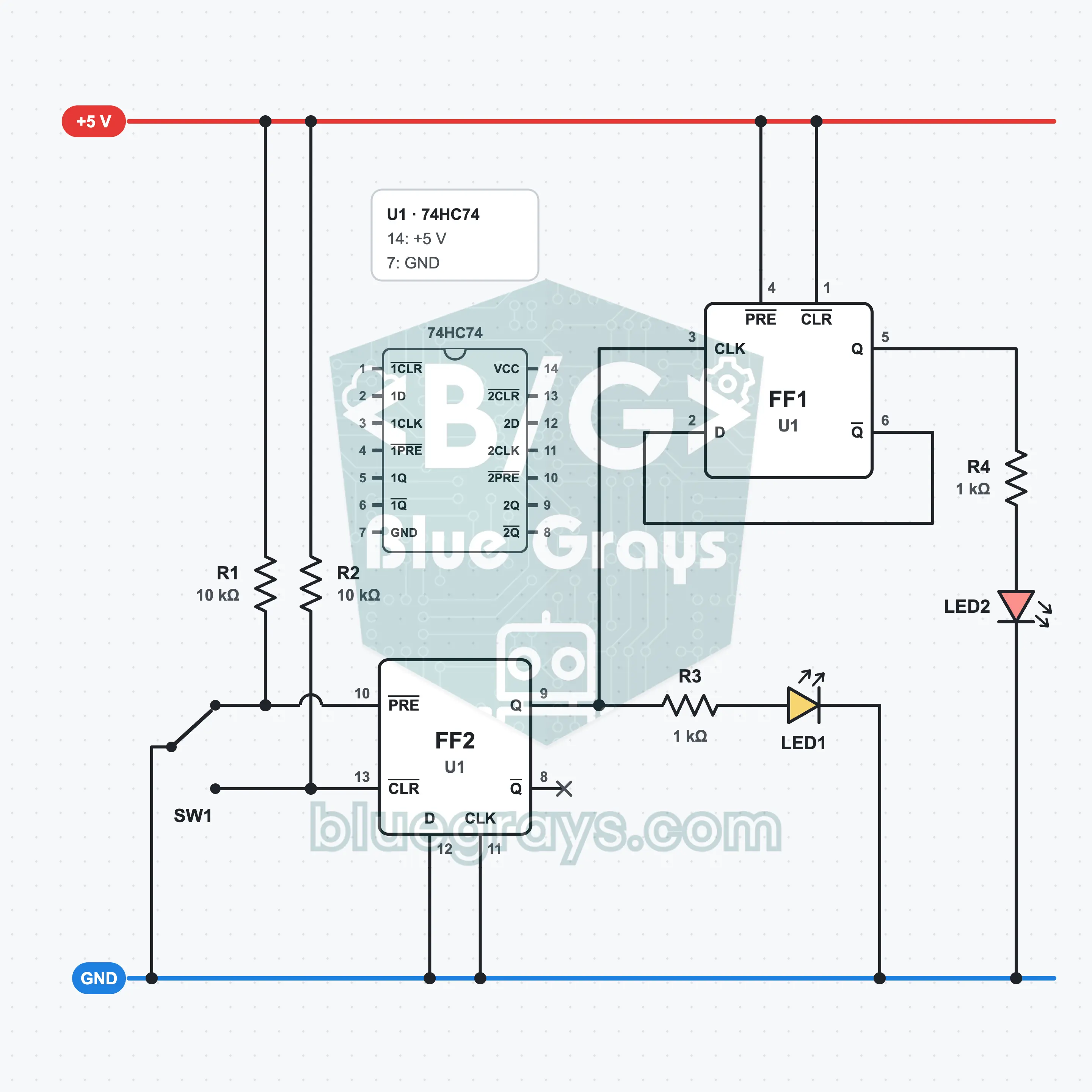
Connect the output of a D flip-flop back to its own input and it becomes a T flip-flop: it changes state on every clock pulse. In the circuit you build with the 74HC74, the yellow LED shows the clock and the red LED shows the output, and the red one flashes at exactly half the speed. This divide-by-two stage is the first stage of every counter and digital clock.
Video
Circuit Diagram
Breadboard Layout
Build Steps
- 1
Plug the MB102 power module onto the end of the breadboard and set both jumper caps to the 5 V position. Leave the module's switch off for now.
- 2
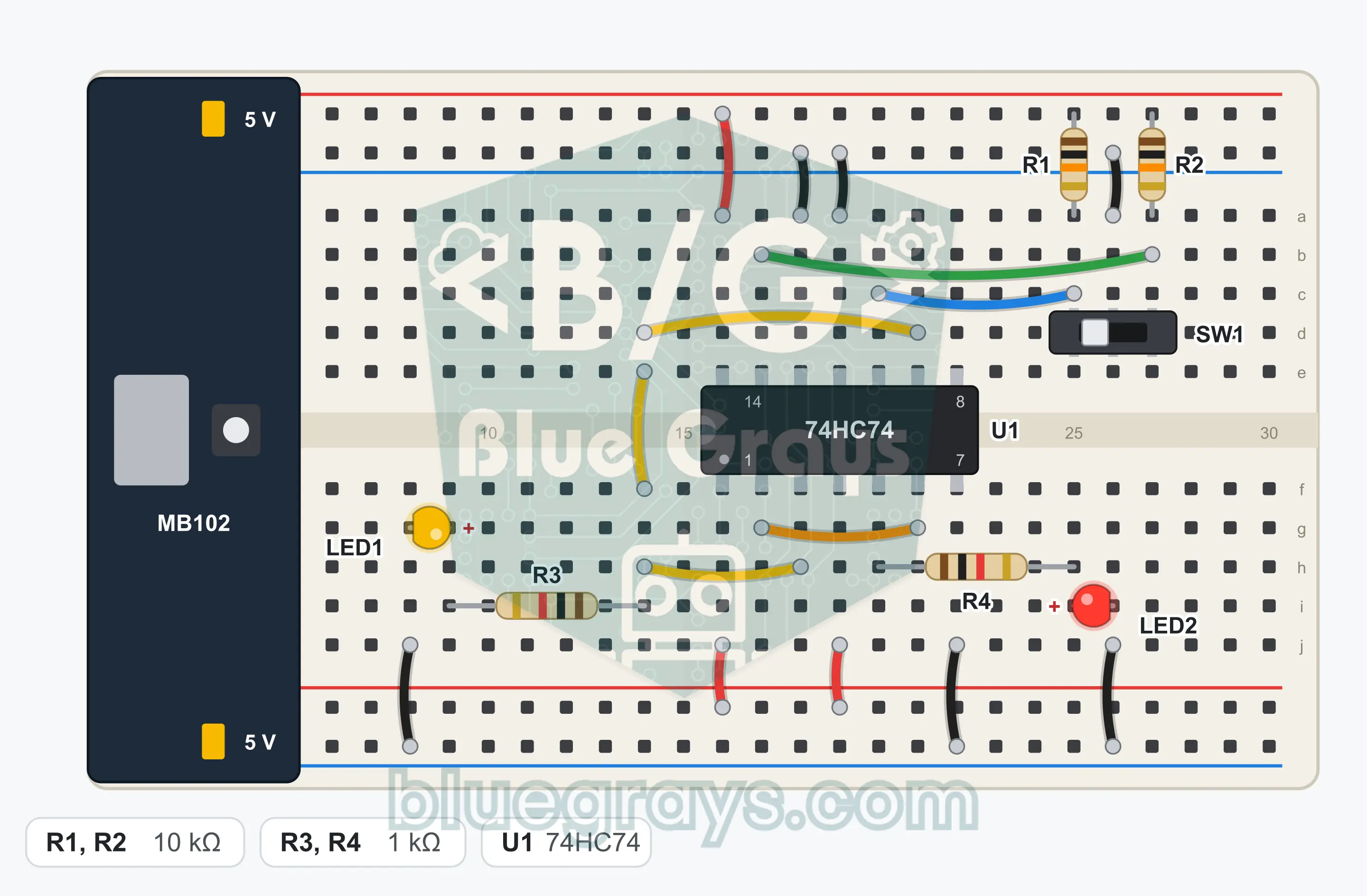
Place the 74HC74 (U1) over the center gap with its notch facing left. The bottom left corner is pin 1; the bottom row runs from 1 to 7 from left to right, and the top row runs from 8 to 14 from right to left.
- 3
Connect pin 14 to the + rail with a jumper wire and pin 7 to the GND (−) rail with a jumper wire.
- 4
Connect pin 4 and pin 1 to the + rail with one jumper wire each. This disables the set and reset inputs of the first flip-flop.
- 5
Connect pin 12 and pin 11 to the GND rail with one jumper wire each.
- 6
Connect pin 6 (Q̄) to pin 2 (D) with a jumper wire. This is the wire that makes the circuit a T flip-flop.
- 7
Connect pin 9 to pin 3 with a jumper wire. The clock pulse travels through this wire.
- 8
Plug in the slide switch (SW1) so that its three legs sit in three separate rows. Connect its middle leg to the GND rail with a jumper wire.
- 9
Connect one outer leg of SW1 to pin 10 with a jumper wire. Fit R1 (10 kΩ) between pin 10 and the + rail. Let's call this side of the switch the 1 position.
- 10
Connect the other outer leg of SW1 to pin 13 with a jumper wire. Fit R2 (10 kΩ) between pin 13 and the + rail. This side is the 0 position.
- 11
Fit R3 (1 kΩ): one end into the row of pin 9, the other end into an empty row.
- 12
Fit LED1 (yellow): long leg (anode) into the row of R3's free end, short leg (cathode) into the GND rail.
- 13
Fit R4 (1 kΩ): one end into the row of pin 5, the other end into an empty row.
- 14
Fit LED2 (red): long leg (anode) into the row of R4's free end, short leg (cathode) into the GND rail. Pin 8 stays unconnected.
- 15
Compare the connections with the schematic, move SW1 to the 0 position, then switch on the power module.
Tip: keep the battery or power supply disconnected while wiring.
Test Steps
- 1
Switch on the power module: the yellow LED must be off. The red LED may be on or off; the power-on state is not predictable.
- 2
Slide SW1 to the 1 position: the yellow LED lights and the red LED changes state.
- 3
Move SW1 back to the 0 position: the yellow LED goes out, the red LED does not change.
- 4
Keep sliding SW1 back and forth: while the yellow LED flashes once on every back-and-forth, the red LED must flash once every two.
- 5
While the red LED is off, bring SW1 to the 1 position four times: the red LED must have lit twice and be off again at the end.
How It Works
When the Q̄ output of the 74HC74 is connected to the D input, the flip-flop toggles on every clock pulse. The red LED flashes at exactly half the speed of the yellow clock LED.
From D flip-flop to T flip-flop
A D flip-flop copies the value on its D input to Q on the clock pulse. In this circuit we do not give D any data from outside; we connect it to the flip-flop's own Q̄ output. Because Q̄ is always the inverse of Q, the flip-flop writes its own inverse on every pulse.
One change on every pulse
While Q = 0, Q̄ = 1 and a 1 is waiting on D. When the clock rises, Q becomes 1, Q̄ drops to 0 and now a 0 is waiting on D. On the next rising edge Q becomes 0 again. This cycle goes on forever. The letter T comes from the word toggle, that is, changing state.
The frequency is divided by two
There is only one rising edge in one full cycle of the clock signal. Q, however, needs two changes for one full cycle: it has to become 1 once and 0 once. That is why one cycle of Q lasts as long as two cycles of the clock. The output frequency is exactly half that of the input.
A clean clock pulse
The set (pin 10) and reset (pin 13) inputs of the second flip-flop in the IC are active at 0. Because SW1 connects its middle terminal to GND, the switch makes pin 9 high in the 1 position and low in the 0 position. Even if the switch bounces, the output settles at the first touch. If the bounce were not cleaned up, the red LED would change a random number of times on every slide.
The first stage of counters
If you connect this output to the clock of a second T flip-flop, the frequency is divided by four, and with a third one by eight. When the outputs of flip-flops lined up side by side are read together, they count in binary. The circuit in front of you is the rightmost digit of that counter.
Truth Table
| Clock (SW1) | Previous Q | New Q (red) |
|---|---|---|
| 0 to 1 | 0 | 1 |
| 0 to 1 | 1 | 0 |
| Holding at 0 or 1 | 0 or 1 | No change |
| 1 to 0 | 0 or 1 | No change |
Q toggles only as SW1 moves to the 1 position. Moving the switch back does not affect the output.
Formulas
Output frequency
fout = fclk / 2
Example: If you bring SW1 to the 1 position 2 times a second (2 Hz), the red LED flashes 1 time a second (1 Hz)
n dividers one after another
fout = fclk / 2^n
Example: Watch crystal: 32,768 Hz / 2^15 = 1 Hz. When 15 flip-flops are connected one after another, you get one pulse a second
T flip-flop rule
On the rising edge: Q(new) = Q̄(previous)
Example: If a pulse arrives while Q = 0, Q = 1; if one more pulse arrives, Q = 0
LED current
I = (Vout − VLED) / R4
Example: (5 V − 2 V) / 1 kΩ = 3 mA; below the 4 mA that is the safe limit for a 74HC output
Common Mistakes
The red LED never changes.
The jumper wire between pin 6 and pin 2 is missing or is plugged into pin 5. The feedback is taken from Q̄, that is, from pin 6.
The yellow LED does not light.
The middle leg of SW1 must be at GND; R1 and R2 must pull pin 10 and pin 13 to the + rail.
The two LEDs flash at the same time.
R4 is plugged into the clock line. One end of it must be in the row of pin 5.
The red LED is always on or always off, and the clock pulse has no effect.
Pin 4 or pin 1 may be touching GND. These inputs are active at 0; both are connected to the + rail.
FAQ
Is there a separate IC for the T flip-flop?
Ready-made T flip-flop ICs are hard to find, because making one is very easy. If you connect the Q̄ output of a D flip-flop to its D input, or hold the J and K inputs of a JK flip-flop at 1, you get a T flip-flop. In this circuit we use the first way.
Why does connecting the Q̄ output to D toggle the output?
A D flip-flop copies the value on D to Q on every clock pulse. If you give D the inverse of Q, Q takes its own inverse on every pulse: if it is 0 it becomes 1, if it is 1 it becomes 0. The new Q̄ reaches D right away, but the flip-flop looks at it only on the next rising edge; that is why the circuit works stably.
Where is a divide-by-two stage used in real life?
The crystal in a wristwatch vibrates 32,768 times a second. When this signal passes through 15 divide-by-two stages one after another, you get exactly 1 Hz, that is, one pulse a second. Counters, frequency meters and the clock circuits of processors use the same structure.
Why does the red LED flash more slowly than the yellow one?
The flip-flop changes state only on the rising edge of the clock. When the yellow LED flashes once, a single rising edge occurs and the red LED changes only once: it either lights or goes out. One full flash of the red LED takes two clock pulses.