
How to Design a PCB: Step-by-Step EasyEDA Guide for Beginners
How to design a PCB in EasyEDA: schematic, footprints, placement, trace width, copper pour, DRC, Gerbers and ordering, plus an Arduino Nano board and KiCad.
PCB design means turning a circuit you built with wires on a breadboard into a permanent printed circuit board, where copper traces connect the components. Today you don't need expensive software or a factory for this: with the free EasyEDA you draw the schematic in your browser, design the board, generate the manufacturing files and order with a few clicks; a week or two later you're holding professional-looking boards.
In this guide you'll follow the whole workflow step by step, using a small Arduino Nano based sensor board as the example: drawing the schematic, choosing the right footprint for each part, placing the parts, setting trace width for the current, adding a GND copper pour, hunting for errors with DRC, generating Gerber files, ordering and testing the board when it arrives. At the end we cover the design mistakes beginners make most often and briefly compare EasyEDA with its powerful alternative, KiCad.
What is a PCB and why move from a breadboard to a PCB?
A PCB is made of thin copper layers bonded to a glass-fibre reinforced epoxy (FR-4) sheet. Most hobby boards are two-layer: there's copper on the top and bottom, and the two layers are connected through small plated holes called vias. The green (or other coloured) coating over the copper is the solder mask; it protects the traces and makes solder stick only to the pads. The white lettering on top is the silkscreen layer. A breadboard is ideal for trying things out, but wires work loose with vibration, long jumpers pick up noise and the circuit won't fit in a box. A PCB gives a sturdy, compact, repeatable result that's easy to debug.
| Feature | Breadboard | Perfboard | PCB |
|---|---|---|---|
| Permanence | Temporary, wires work loose | Permanent, soldered by hand | Permanent and sturdy |
| Preparation time | Minutes | Hours (every connection by hand) | A few hours of design, 1–2 weeks for production and shipping |
| Making copies | Rebuild every time | Re-solder every time | As many as you like from the same files |
| Look and size | Large, a tangle of wires | Medium | Small and tidy |
| SMD parts | Not possible | Difficult | Easy |
| Best for | Experimenting and learning | One-off simple circuits | Finished projects, several copies |
Example project: an Arduino Nano based sensor board
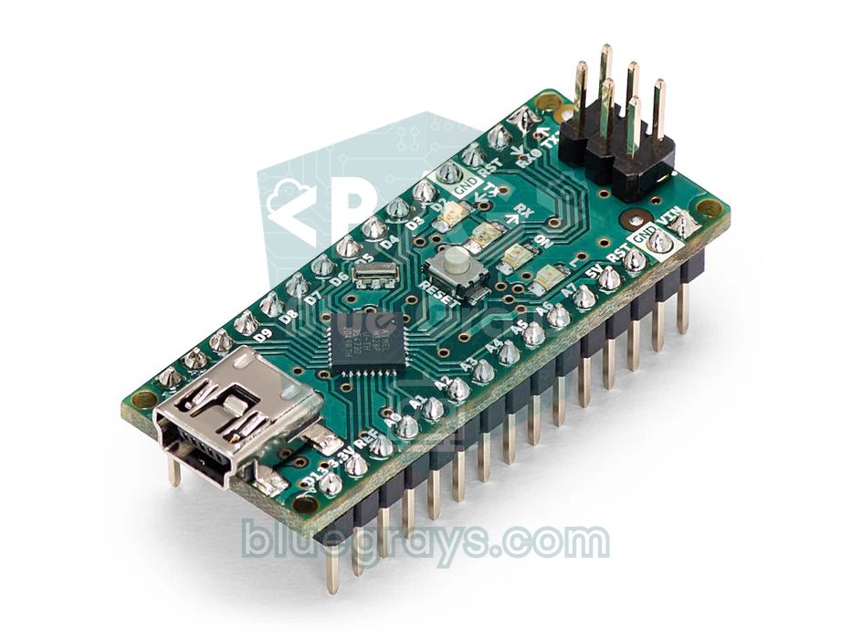
Throughout the guide we'll move a circuit people often build on a breadboard onto a PCB: an Arduino Nano, a DHT22 temperature and humidity sensor, a four-pin header for an I2C OLED display, two buttons, an LED and a passive buzzer. Instead of soldering the Nano directly to the board, we'll plug it into two 15-pin female headers, so you can take it out for another project or replace it easily if it fails. The board will take a 7–12 V adapter through a screw terminal and be protected against reverse polarity with a diode. For pin numbers, see Arduino Nano pinout.
| Ref | Part | Value | Footprint | Nano connection |
|---|---|---|---|---|
| U1 | Arduino Nano (on female headers) | - | 2 × 1×15 female header, 2.54 mm, rows 15.24 mm apart | - |
| U2 | DHT22 sensor | - | 1×4 pin, 2.54 mm | D2 (data), 5V, GND |
| R1 | Pull-up resistor | 10 kΩ | Axial THT, 10.16 mm pitch | Between D2 and 5V |
| J1 | OLED header | GND, VCC, SCL, SDA | 1×4 female header, 2.54 mm | A5 (SCL), A4 (SDA), 5V, GND |
| SW1, SW2 | Button | 6 × 6 mm | 4-pin THT tact switch | D3 and D4, other side to GND |
| D2 | LED | 5 mm red | LED 5 mm, 2.54 mm pitch | D6 |
| R2 | LED resistor | 330 Ω | Axial THT, 10.16 mm pitch | Between D6 and the LED |
| BZ1 | Passive buzzer | 12 mm | Buzzer 12 mm, 7.6 mm pitch | D8 |
| D1 | Schottky diode | 1N5819 | DO-41 axial | Between terminal + and VIN |
| C1 | Electrolytic capacitor | 100 µF / 25 V | Radial, 2.5 mm pitch | Between VIN and GND |
| J2 | Screw terminal | 2-pin | 5.08 mm pitch | 7–12 V input |
PCB design workflow: 7 steps
- Schematic: Draw the circuit with symbols and check every connection.
- Footprints: Choose the pad and hole layout each symbol will occupy on the board.
- Placement: Set the board size and place the parts in logical groups.
- Traces: Draw the connections as copper traces; keep power traces wide.
- Copper pour: Fill the empty areas with copper connected to GND.
- DRC: Check the design rules and fix the errors.
- Gerber and ordering: Generate the manufacturing files, check them and upload them to a manufacturer.
1. Drawing the schematic in EasyEDA
EasyEDA comes in two editions: the older, simpler Standard and the newer, more powerful Pro. Both are free and run in the browser or as a downloadable desktop client. If you're starting out, start with Pro. After creating a free account, make a new project; when it opens you get an empty schematic sheet. Search the Library panel for the part name or its LCSC part number and place it on the schematic; basic parts such as resistors, capacitors and LEDs come with a ready-made symbol and footprint. Then connect the pins with the Wire tool and use the VCC and GND symbols for power. If you're not used to reading schematics, How to read a circuit diagram explains the symbols one by one.
2. Choosing footprints: the symbol's counterpart on the board
The symbol shows what a part does in the schematic; the footprint defines the pads and holes its legs sit in on the board and the area it takes up. The same 10 kΩ resistor has dozens of footprints: a through-hole (THT) axial resistor with 7.62 mm or 10.16 mm pitch, or surface-mount (SMD) packages such as 0805 and 0603. Never pick a footprint without checking the dimensions of the part in your hand with a ruler or calipers. For your first board, it's best to start with THT parts that are easy to solder by hand; when you move to SMD, the 0805 size is the most comfortable to solder by hand. For the codes printed on SMD resistors, use the SMD Code Decoder tool.
| Part | Common footprint | Critical dimension | Note |
|---|---|---|---|
| 1/4 W resistor | Axial THT | 7.62 mm (300 mil) or 10.16 mm (400 mil) pitch | 10.16 mm makes bending the legs easy |
| 5 mm LED | LED-5MM | 2.54 mm pitch | The flat edge and short leg are the cathode; mark it on the silkscreen |
| Pin header | 1×N, 2.54 mm | 1.0 mm hole | For the Nano, 15.24 mm between the two rows |
| Electrolytic capacitor | Radial | 2.0 / 2.5 / 3.5 mm pitch depending on diameter | Mark the positive lead on the silkscreen |
| Screw terminal | 2-pin | 5.08 mm or 3.5 mm pitch | Make the wire entry face the board edge |
| Tact button | 6 × 6 mm THT | 6.5 × 4.5 mm hole pattern | Pairs of opposite pins are connected internally |
| SMD resistor / capacitor | 0805, 0603 | 0805 = 2.0 × 1.25 mm | 0805 and larger for hand soldering |
3. Board size and placement
- Outline first: Draw the board outline. Our example board is 60 × 50 mm; many manufacturers make boards under 100 × 100 mm in their cheapest price bracket.
- Mounting holes: Put 3.2 mm (M3) holes in the four corners, about 3.5 mm in from the edge; screwing the board into a box becomes much easier later.
- Connectors at the edge: Make the screw terminal, the OLED header and the Nano's USB socket face the board edge, so parts don't get in the way when plugging in cables.
- Group your placement: Keep the power parts (terminal, diode, capacitor) in one corner and the buttons on the edge where the user will press them.
- Keep the sensor away from heat: Place the DHT22 away from the Nano's regulator and the buzzer; the regulator's heat can throw the temperature reading off by a few degrees.
- Leave room for soldering: Leave enough space between parts for the soldering iron tip; don't let the gap between two neighbouring pads drop below 1 mm.
- Silkscreen: Write each part's reference (R1, D1), the LED and capacitor polarities, the pin names and the board's name; don't let text run over the pads.
4. Routing traces and choosing trace width
When placement is finished you'll see thin lines between the parts; these ratsnest lines show connections that exist in the schematic but haven't been made in copper yet. You turn each one into a copper trace with the Track tool. A trace's width sets how much current it can carry: a narrow trace heats up at high current, causes voltage drop and in the worst case burns out. 0.25–0.3 mm is enough for signal traces; keep power traces such as 5 V and VIN at least 0.6–1 mm wide, especially if they'll feed servos, motors or LED strips. The values below are rough figures calculated with the IPC-2221 approximation for an outer layer with 1 oz (35 µm) copper and about 10 °C of temperature rise; leaving a safety margin is always a good idea.
| Trace width | mil | Approximate current (1 oz, outer layer, 10 °C) | Use |
|---|---|---|---|
| 0.25 mm | 10 mil | ≈ 0.9 A | Signal traces |
| 0.5 mm | 20 mil | ≈ 1.5 A | Logic power, sensors |
| 1.0 mm | 40 mil | ≈ 2.4 A | Power for servos, relays, small motors |
| 2.0 mm | 80 mil | ≈ 4 A | High-current power traces |
Keep the gap between traces (clearance) at least 0.2–0.3 mm; most manufacturers can make tighter gaps, but a wide gap leaves room for error in both manufacturing and soldering. When a trace has to move to the other layer, use a via; a via with a 0.3 mm hole and 0.6 mm outer diameter is a standard choice for hobby boards. Turn corners with 45-degree bends and avoid sharp angles (less than 90 degrees). On two-layer boards, running traces mostly horizontally on the top layer and vertically on the bottom makes crossings easier to solve. To work out the LED resistor value, use the LED Resistor Calculator tool.
5. GND copper pour
Once all the traces are drawn, fill the remaining empty surface of the board with copper connected to the GND net; in EasyEDA the Copper Area tool does this. Add the copper pour to both the top and bottom layers and tie the two layers together with a few GND vias scattered across the board. This has three benefits: every part's GND connection is made the short way without drawing separate traces, the resistance and noise of the ground path drop, and less copper has to be etched away by the manufacturer. The GND pads of through-hole parts connect to the pour with thermal reliefs (four thin spokes), so the soldering iron can heat the pad without losing its heat into the large copper area. After adding the pour, rebuild it and remove any small copper islands that aren't connected to anything.
6. Running the DRC
DRC (Design Rule Check) is the tool that automatically scans your design against the rules you set: it lists traces that are too close together, copper too near the edge, overlapping pads, parts sticking out of the board and nets that still aren't connected. Click any line in the error list and EasyEDA shows you the problem spot. Run the DRC until no errors remain, but don't rely on it alone; DRC can't know that a footprint was chosen wrongly or that a pin was connected to the wrong net. Also do these checks by hand before ordering:
- Make sure no ratsnest lines remain on screen and the DRC reports zero errors.
- Print the board on paper at 100% scale and lay the real parts on the paper; the hole spacings and the Nano headers should match exactly.
- Open the 3D view: check that parts don't overlap and that the USB socket and terminal face the edge.
- Follow the power path: are the terminal, diode, capacitor and the Nano's VIN pin in the right order?
- Check that the silkscreen has polarity marks, pin names, the board name and a version number (e.g. v1.0).
7. Generating Gerber files and ordering
Manufacturers don't work with your design file but with industry-standard Gerber files. Gerber describes each layer of the board in a separate file; hole positions and diameters go in a separate drill file. When you choose the Gerber output in EasyEDA's fabrication menu, all the files are put into a single ZIP archive; the option to order directly from EasyEDA's sister manufacturer is on this screen too. You can also upload the ZIP to any other manufacturer. Whichever you choose, after uploading, inspect your board layer by layer in the online Gerber viewer; this is your last chance to see that what you drew is what will be made.
| File (extension) | Contents |
|---|---|
| GTL / GBL | Top and bottom copper layers |
| GTS / GBS | Top and bottom solder mask (where pads stay exposed) |
| GTO / GBO | Top and bottom silkscreen text |
| GKO or GM1 | Board outline and internal cut-outs |
| DRL / TXT | Hole positions and diameters |
| Order setting | Recommended for a hobby board | Explanation |
|---|---|---|
| Layers | 2 | Enough for almost all boards of this kind |
| Board thickness | 1.6 mm | The standard thickness, cheapest and sturdiest option |
| Copper weight | 1 oz (35 µm) | Enough unless you have high currents |
| Surface finish | Lead-free HASL | Cheap and easy to solder; ENIG has a flatter surface for fine-pitch SMD parts |
| Solder mask colour | Green | The fastest and cheapest colour at most manufacturers |
| Quantity | 5 | The minimum at most manufacturers; spares come in handy if something goes wrong |
Boards are usually made within a few days, while shipping can take a week or two depending on the method you choose. When the boards arrive, don't solder everything at once: first fit only the diode, capacitor and terminal, measure with a multimeter that there's no short between VIN and GND, then power it up and confirm you see the right voltage on the Nano's header. Then solder the parts from lowest to tallest: resistors, diode, buttons, headers and finally the big parts. For clean joints see How to solder, and for measuring see How to use a multimeter. Plug in the Nano and upload the test sketch below to check every connection on the board one by one.
1// Nano kartı ilk test: her bağlantıyı tek tek doğrula
2// Nano board first test: check every connection one by one
3#include <Wire.h>
4
5const int DHT_PIN  = 2;              // DHT22 veri hattı, 10 kΩ pull-up / DHT22 data line, 10 kΩ pull-up
6const int BUTON1   = 3;              // buton GND'ye / button to GND
7const int BUTON2   = 4;
8const int LED_PIN  = 6;              // LED + 330 Ω
9const int BUZZER   = 8;              // pasif buzzer / passive buzzer
10
11void i2cTara() {
12  byte bulunan = 0;
13  for (byte adres = 1; adres < 127; adres++) {
14    Wire.beginTransmission(adres);
15    if (Wire.endTransmission() == 0) {             // cihaz cevap verdi / a device answered
16      Serial.print(F("I2C cihaz / device: 0x"));
17      Serial.println(adres, HEX);                  // OLED genelde 0x3C / OLED is usually 0x3C
18      bulunan++;
19    }
20  }
21  if (bulunan == 0) Serial.println(F("I2C cihaz yok: A4/A5 yollarini kontrol et / no I2C device: check the A4/A5 tracks"));
22}
23
24void setup() {
25  Serial.begin(9600);
26  pinMode(BUTON1, INPUT_PULLUP);
27  pinMode(BUTON2, INPUT_PULLUP);
28  pinMode(LED_PIN, OUTPUT);
29  pinMode(DHT_PIN, INPUT);
30  Wire.begin();
31
32  Serial.println(F("--- Kart testi / board test ---"));
33  i2cTara();
34  // Pull-up direnci lehimliyse veri hattı boşta HIGH okunur
35  // If the pull-up resistor is soldered, the idle data line reads HIGH
36  Serial.print(F("DHT hatti / DHT line: "));
37  Serial.println(digitalRead(DHT_PIN) ? F("HIGH (pull-up tamam / OK)") : F("LOW (pull-up ya da kisa devre? / pull-up or short?)"));
38  tone(BUZZER, 2000, 150);                         // buzzer kısa bip / short beep
39}
40
41void loop() {
42  digitalWrite(LED_PIN, (millis() / 500) % 2);     // LED yarım saniyede bir / LED every half second
43
44  static bool once1 = HIGH, once2 = HIGH;
45  bool b1 = digitalRead(BUTON1);
46  bool b2 = digitalRead(BUTON2);
47  if (b1 == LOW && once1 == HIGH) { Serial.println(F("Buton 1 / button 1")); tone(BUZZER, 1000, 80); }
48  if (b2 == LOW && once2 == HIGH) { Serial.println(F("Buton 2 / button 2")); tone(BUZZER, 1500, 80); }
49  once1 = b1;
50  once2 = b2;
51  delay(20);                                       // basit debounce / simple debounce
52}
At startup the code scans the I2C bus and, if the OLED is plugged in, prints its address (usually 0x3C); if nothing is found, it tells you to check the A4 and A5 traces. If the R1 pull-up resistor is soldered correctly, the DHT22 data line reads HIGH when idle; if you see LOW, the resistor is missing or the line is shorted to GND. The buzzer gives a short beep at startup, the LED blinks every half second and each button prints its name to the Serial Monitor and makes a different sound. Once all these tests pass, you can add the sensor and display libraries and move on to your actual project.
Common PCB design mistakes
| Mistake | Result | Prevention |
|---|---|---|
| Wrong footprint or pin order | The part won't fit or is connected backwards | Check the datasheet, try the part on a 100% scale printout |
| Wrong spacing between the Nano headers | The Nano won't sit in the headers | Rows must be 15.24 mm apart with 2.54 mm pin pitch |
| Thin power traces | Heating, voltage drop, resets | Keep power traces at 0.6–1 mm or wider |
| GND pour not assigned to the net | There's a copper pour, but it isn't connected to any pad | Set the pour's net to GND and rebuild it |
| Forgetting mounting holes | The board can't be screwed into a box | Place M3 holes in the corners from the start |
| Silkscreen over the pads | Text is unreadable and soldering gets harder | Keep text away from pads, use at least 0.8 mm text height |
| No polarity marks | The LED, diode or capacitor gets fitted backwards | Mark the cathode, the plus side and pin 1 on the silkscreen |
| Connector facing into the board | Cables can't be plugged in, the USB socket is blocked | Check connector directions in the 3D view |
A quick look at KiCad: EasyEDA or KiCad?
| Feature | EasyEDA | KiCad |
|---|---|---|
| Price | Free | Free and open source |
| How it works | Browser or desktop client, projects in your account | Entirely on your computer, no internet needed |
| Parts library | Linked to the LCSC catalogue, symbols and footprints ready | Large official library; you add missing parts yourself |
| Learning | Quick start, simple interface | More settings, a bit longer to learn |
| Ordering | In one step from inside the app | You export Gerber and drill files and upload them to a manufacturer |
| Advanced features | More than enough for hobby and small projects | Many layers, differential pairs, length matching, SPICE simulation |
| 3D view | Yes | Yes, with STEP export |
In KiCad the workflow is the same: you draw the circuit in the Schematic Editor, assign a footprint to each symbol, do placement and routing in the PCB Editor, run the DRC and produce Gerber and drill files from the Plot menu. For your first board, EasyEDA's ready-made library and one-step ordering save time. As your designs grow, moving to KiCad makes sense if you want to work offline, keep your files entirely to yourself and use advanced features; the footprint, trace width, copper pour and DRC concepts you've learned here are the same in both programs.
The moment you hold your first PCB, you'll see a sturdy, repeatable board taking the place of the tangle of wires on your breadboard; even if you make a mistake, the second version is always better. Start with a small board with THT parts, double-check the footprints and power traces, and print it on paper to try the parts before ordering. The wiring diagrams of the LED, button, buzzer, DHT11, LCD and OLED projects in the BlueGrays app make a good starting point when designing your own board; get the circuit working on a breadboard with the app's steps first, then move it to a PCB.
Frequently asked questions
How do you design a PCB?
First you draw the circuit as a schematic in a program such as EasyEDA or KiCad, then you assign a footprint to each part, place them on the board and draw the connections as copper traces. After filling the empty areas with GND copper and checking for errors with the DRC, you generate the Gerber files and upload them to a PCB manufacturer.
Is EasyEDA free?
Yes. Both the Standard and Pro editions of EasyEDA are free and can be used in the browser or with the downloadable desktop client. You only need to create a free account; having your boards made is a separate service you pay the manufacturer of your choice for.
What is a Gerber file?
Gerber is the standard file format PCB manufacturers use. Each layer of the board (copper, solder mask, silkscreen, outline) is described in its own Gerber file, and the hole positions in a separate drill file. EasyEDA and KiCad create these files in a few clicks, and they're usually uploaded as a single ZIP archive.
How wide should PCB traces be?
0.25–0.3 mm is enough for signal traces. Widen power traces according to the current they'll carry: on an outer layer with 1 oz copper, about 0.5 mm carries around 1.5 A and 1 mm around 2.4 A. For traces feeding servos, motors and LED strips, use 1 mm or more to leave a safety margin.
Which is better, EasyEDA or KiCad?
EasyEDA is faster for beginners: the parts library is ready and you order from inside the program. KiCad is an open-source program that runs entirely locally and has more advanced features. Since the basic concepts are the same, it's easy to start with EasyEDA and move to KiCad later.
How long does a PCB order take and what's the minimum quantity?
Most manufacturers make standard two-layer boards within a few days; the shipping method is what really sets the total time, usually a week or two. The minimum order at most manufacturers is 5 boards, and for small boards the price difference between 5 and 10 pieces is usually small.
Projects to build after reading this
See all projects
LED Blink
The very first hello of electronics: switching a single LED on and off. The Arduino turns the LED on and off at short intervals, so the light blinks quickly. You see in the simplest way how the board

LED Control with a Push Button (Push)
Just like a doorbell: the light stays on as long as you press, and goes off when you let go. The Arduino keeps listening to the button; while it's pressed the LED is on, and the moment you lift your f
Using a Buzzer
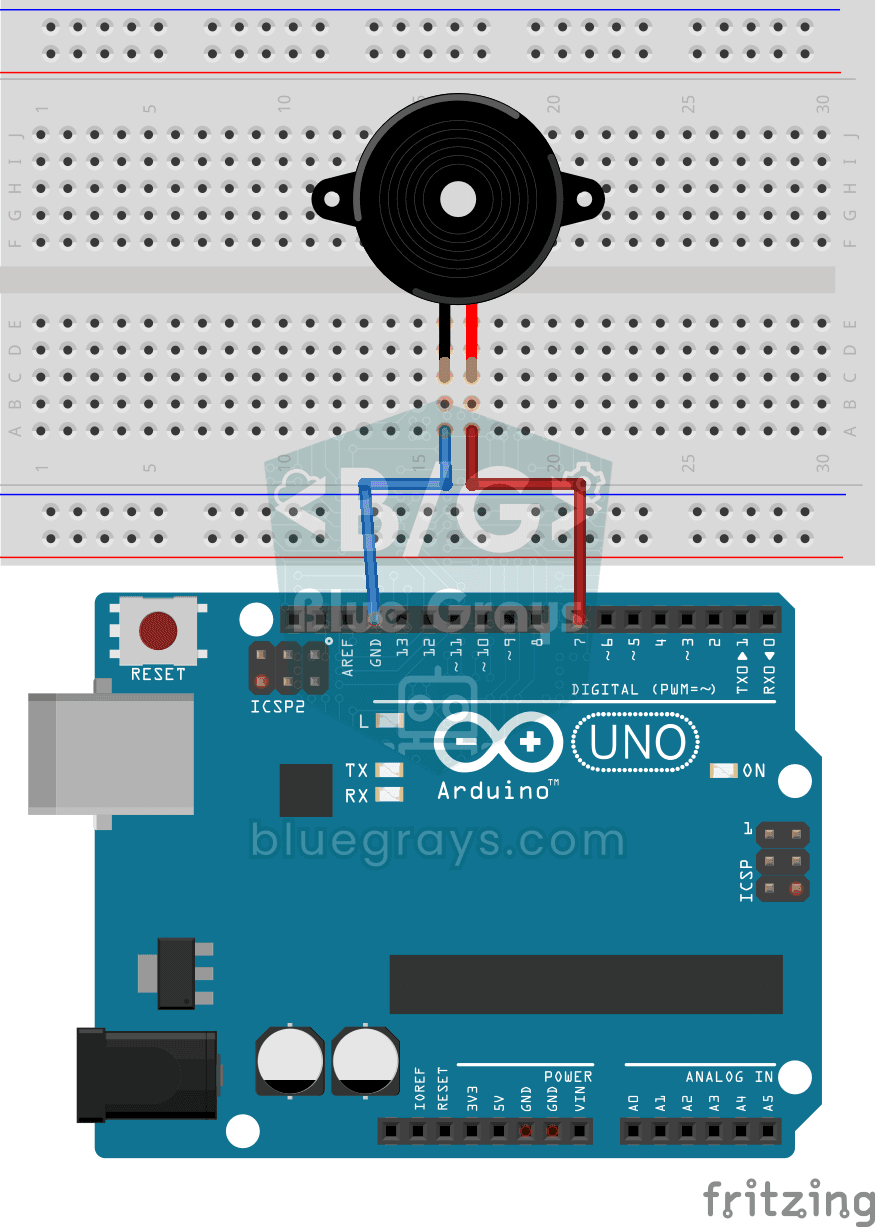
Ever wondered how a doorbell or an alarm makes its sound? The Arduino makes a small buzzer beep at short intervals: beep, pause, beep, pause. You see how sound is made with electricity and take the fi
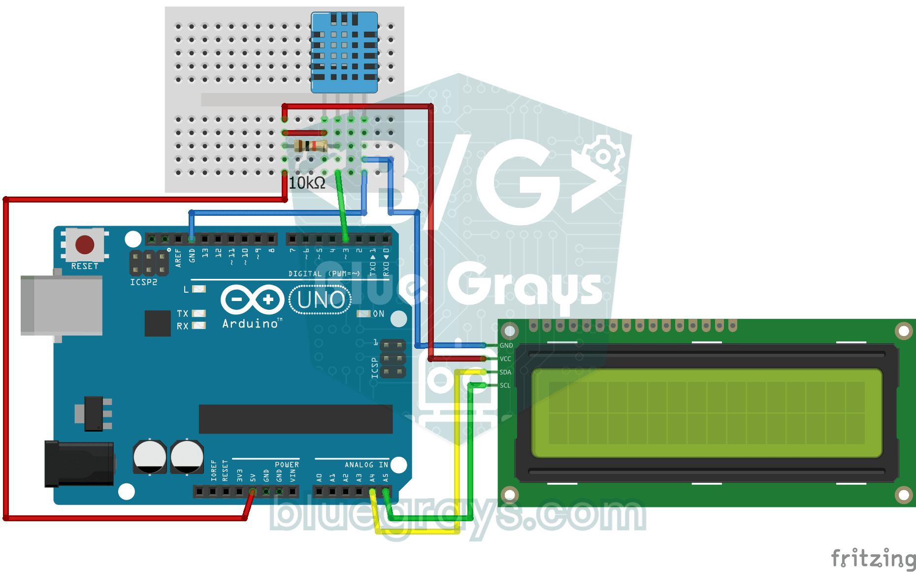
Temperature and Humidity with DHT11
How warm is your room, and is the air humid or dry? The DHT11 sensor measures temperature and humidity, and the Arduino writes the values on a two-line LCD screen, refreshing every couple of seconds.
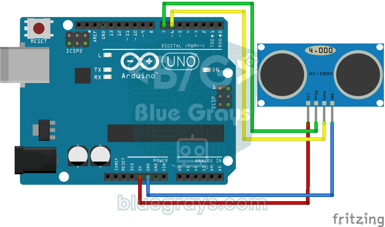
HC-SR04 Distance Measurement (Serial Display)
The HC-SR04 sensor works just like a bat finding its way in the dark: it sends out a sound you cannot hear, listens for the echo and measures how far away the object in front of it is. The Arduino wri
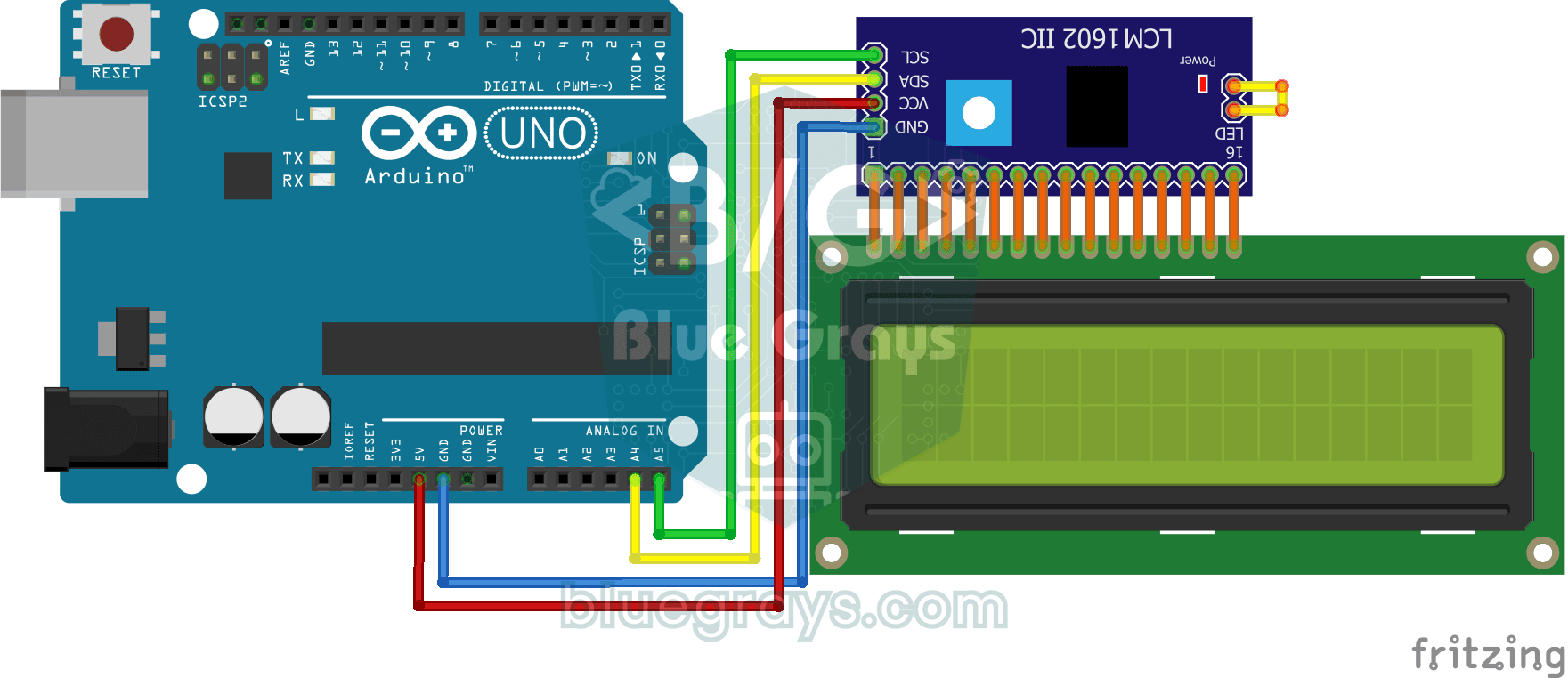
Using LCD Screen with I2C
Give your Arduino its own screen and make it write its first message. The two-line LCD screen hooks up with just a few wires; a greeting appears on the top line, then a second message on the bottom li

Paddle Ball Game - SSD1306
A ball, two paddles and you: you play table tennis, one of the very first video games, on a small OLED screen. Two buttons move your paddle on the right up and down, while the computer controls the le

Smart Electronic Safe
A small safe for your valuables that opens with a code. You type your four-digit code on the keypad; if it is right, the servo motor opens the lock, the green light comes on and the screen shows the s